


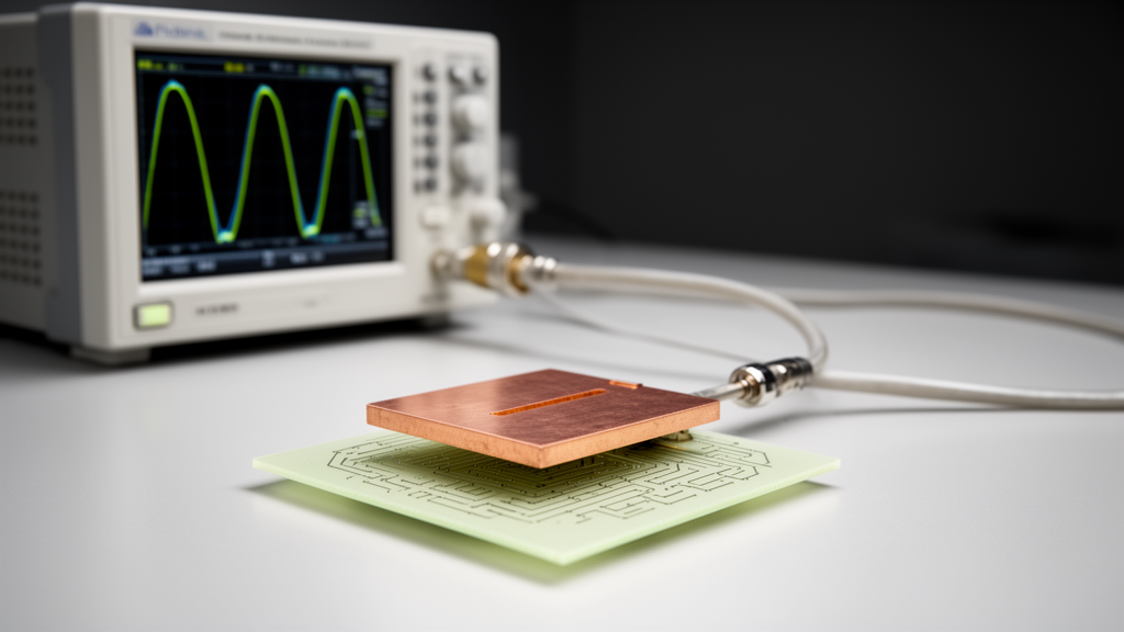
A compact antenna measuring just 20 by 20 millimetres has been designed, fabricated and experimentally tested to operate across three distinct wireless bands at approximately 2.4 GHz, 6 GHz and 8 GHz, according to a study published in the journal Advanced Metamaterials. The device, a coplanar waveguide-fed microstrip patch antenna, combines an E-shaped slot etched into the radiating patch with a T-shaped defected ground structure, and achieved a maximum realized gain of 5.4 dBi in measurements while keeping the reflection coefficient below the −10 dB impedance-matching threshold in all three operating bands.
The antenna was built on a low-cost FR-4 substrate with a relative permittivity of 4.4, a loss tangent of 0.02 and a thickness of 1.6 millimetres, giving overall dimensions of 20 × 20 × 1.6 mm³. The researchers, Touko Tcheutou Stephane Borel and Rashmi Priyadarshini, chose the coplanar waveguide feeding technique because it offers simple fabrication, reduced radiation leakage and easy integration with radio-frequency circuits, advantages that matter when a planar antenna must sit alongside other circuit elements in a compact wireless device.
What distinguishes the work is its incremental design methodology. The team began with a conventional CPW-fed rectangular patch as a reference configuration, then introduced the E-shaped slot into the radiating element, and finally etched T-shaped slots into the ground plane to create the defected ground structure. This stepwise approach allowed the authors to isolate the contribution of each modification to the antenna’s resonant frequencies, impedance matching and radiation properties, an aspect they argue is not well explained in much of the existing literature, where comparisons between designs tend to be qualitative rather than quantitative.
The simulation results traced a clear progression. The basic CPW-fed patch exhibited two resonances, near 2.4 GHz and 8 GHz, but its impedance matching was limited, with reflection coefficient values approaching the −10 dB threshold. Adding the E-shaped slot retained those two resonances while significantly improving matching, because the slot alters the surface current distribution across the radiating area and lengthens the effective current path. The decisive change came with the T-shaped slots in the ground plane: the defected ground structure redistributed current in the ground, intensified electromagnetic coupling between the radiating element and the feed line, and generated an additional resonant mode near 6 GHz, completing the tri-band response.
The resonance near 6 GHz proved to be the deepest of the three, with the reflection coefficient reaching values close to −30 dB, indicating excellent impedance matching at that frequency. The resonances around 2.4 GHz and 8 GHz also remained below the −10 dB criterion. All designs were optimized using an iterative parametric approach in ANSYS HFSS, with initial dimensions calculated from standard transmission-line model equations before full-wave electromagnetic simulation refined the geometry.
Parametric analysis clarified which structural feature controls which behaviour. Varying the T-slot length primarily affected impedance matching: at T = 1.0 mm the reflection coefficient stayed predominantly above −10 dB with shallow, poorly defined resonant dips, while T = 1.5 mm produced clear resonances with S11 values well below −10 dB. Increasing T further to 2.0 mm degraded performance, making the resonances less stable and slightly distorted. The E-slot length, by contrast, mainly tuned the resonant frequencies: at E = 2.0 mm the resonances shifted toward higher frequencies as the effective current path shortened, while E = 3.0 mm pushed them lower. The combination of E = 2.5 mm and T = 1.5 mm delivered the most balanced performance and was selected as the optimal design.
Simulated gain improved steadily across the design evolution. The simple CPW-fed antenna achieved gains between 1 dB and 2.7 dB, the E-slot version improved this by roughly 4 dB at the main operating frequencies, and the final E-slot-plus-DGS design reached approximately 5.4 dB near 6 GHz while staying above 2 dB across most of the operating range. The authors attribute the improvement to the combined effect of the two modifications, which adjust the surface current distribution and reduce unwanted current losses within the ground plane. Radiation patterns, examined at 2.6 GHz, 6.4 GHz and 8.29 GHz, showed a bidirectional pattern in the E-plane and a nearly omnidirectional pattern in the H-plane, with the antenna maintaining a dominant co-polarized component and low cross-polarization throughout.
To validate the design experimentally, the team fabricated a prototype on the same FR-4 substrate using conventional printed circuit board techniques and measured its reflection coefficient with a vector network analyzer. The measured response confirmed tri-band behaviour consistent with the simulations, with resonances near 2.4 GHz, 6 GHz and 8 GHz and the deepest dip around 6 GHz. A slight shift between the simulated and measured curves was attributed to fabrication tolerances, losses associated with the FR-4 substrate, connector and soldering effects, and minor variations in the substrate’s dielectric constant, but the authors describe the overall agreement as very good.
The impedance measurements reinforced that picture. The measured voltage standing wave ratio approached 1 near the 6 GHz resonance, indicating optimal matching, and remained within acceptable limits around 2.4 GHz and 8 GHz. On the Smith chart, spanning 1 GHz to 10 GHz, the impedance trajectory circulated near the centre of the chart, and at the marked resonant frequency the measured input impedance was approximately 46.4 + j0.5 ohms, close to the standard 50-ohm characteristic impedance and almost purely resistive at resonance.
Measured gain and radiation efficiency followed the simulated trends closely. The gain reached about 5.4 dB near 6 GHz, approximately 3 dB in the lower band at 2.4 GHz and above 4 dB in the higher band at 8 GHz, while radiation efficiency peaked at around 94 percent, 86 percent and 85 percent at 2.4, 6 and 8 GHz respectively, a notable result given the lossy nature of the FR-4 substrate. The authors report that the antenna maintains stable radiation characteristics across all operating bands and, in a quantitative comparison with recently reported designs, offers a favourable compromise among size, multi-band operation and radiation performance. They suggest the compact tri-band structure could find use in future wireless communication applications such as WLAN and broadband systems, though the study reports antenna performance measurements rather than deployment in any specific device or standard.
Subject of Research: Design and experimental validation of a compact tri-band CPW-fed E-slotted microstrip patch antenna with a T-shaped defected ground structure.
Article Title: Design of a CPW-Fed E-slotted patch antenna with defected ground structure for wireless applications
Article References: Stephane Borel, T. T., & Priyadarshini, R. (2026). Design of a CPW-Fed E-slotted patch antenna with defected ground structure for wireless applications. Advanced Metamaterials, 2(1), Article 1. https://doi.org/10.1007/s44468-026-00005-5
Image Credits: AI Generated
DOI: 10.1007/s44468-026-00005-5
Keywords: microstrip patch antenna, CPW feed, defected ground structure, tri-band antenna, E-shaped slot, FR-4 substrate, impedance matching, reflection coefficient, VSWR, radiation efficiency, ANSYS HFSS, wireless communications
News Source: Denise Maddox. (October 27, 2026). Compact E-Slotted Patch Antenna with Defected Ground Delivers Tri-Band Wireless Performance. Scienmag.