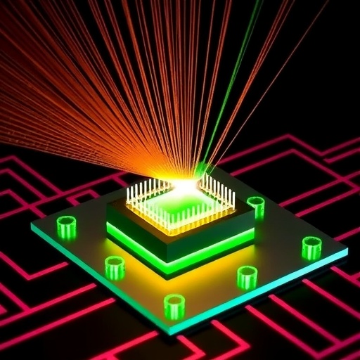
In a groundbreaking advancement published in the latest issue of Opto-Electronic Science, a team of researchers has unveiled an innovative photoconductive semiconductor switch (PCSS) that leverages a novel phonon-assisted absorption mechanism within gallium oxide (Ga₂O₃) crystals. This development stands to revolutionize high-power microwave (HPM) systems, particularly for low-altitude security applications such as the defense of civil airports against non-cooperative drone threats. The newly fabricated switch astonishingly reaches a voltage conversion efficiency of 98.93%, ushering in a new era for compact, efficient, and robust electronic defense technologies.
The rapidly evolving low-altitude economy has introduced unprecedented challenges for security systems, especially in protecting critical infrastructure and urban airspaces from unauthorized drone intrusions. Current methods rely heavily on high-power microwave technology, which disrupts or damages hostile drone electronics through focused electromagnetic radiation. The PCSS at the heart of these systems plays a pivotal role, fundamentally influencing key performance parameters such as voltage endurance, energy conversion efficiency, and output power density. Improvements in PCSS technology dramatically impact the miniaturization and operational capability of HPM systems, marking the progress toward real-world, deployable solutions.
Historically, gallium arsenide (GaAs)-based PCSS devices formed the backbone of photoconductive switches but were constrained by their limited breakdown field strength and diminished capacity to withstand high voltages. These material limitations inhibited efforts to develop smaller, more powerful switches required for the stringent demands of modern HPM applications. As an alternative, gallium oxide (Ga₂O₃), an ultra-wide bandgap semiconductor, promises significantly higher voltage endurance and thermal stability, offering a promising material platform. However, conventional Ga₂O₃-based PCSSs have suffered from poor voltage conversion efficiencies and excessive loss during operation, primarily due to reliance on impurity-level absorption as the excitation method.
The breakthrough spearheaded by Professor Wei Zheng and his team at Sun Yat-sen University addresses these longstanding issues through the introduction of a phonon-assisted absorption mechanism. This fundamentally different carrier excitation process harnesses lattice vibrations (phonons) to facilitate efficient electron transitions inside Ga₂O₃, circumventing the inefficiencies tied to impurity-based excitation. This pioneering approach was supported by collaborating institutions: the Shanghai Institute of Optics and Fine Mechanics, which provided ultrahigh-quality Fe-doped Ga₂O₃ single crystals, and the Shanghai Institute of Laser Plasma, which contributed critical high-power testing and validation in realistic scenarios.
A defining advantage of Ga₂O₃ lies in its high breakdown field strength, far surpassing traditional semiconductor materials like GaAs and silicon carbide (SiC). This intrinsic property enables devices fabricated from Ga₂O₃ to endure significantly larger voltages without failure, laying the foundation for high-voltage capability switches essential for cutting-edge HPM systems. Experimentally, the newly developed PCSS demonstrated a peak output voltage close to the 4000 V bias threshold, reaching 3957 V and thus achieving nearly ideal voltage conversion efficiency near 99%, an unprecedented figure in this realm.
In addition to its voltage resilience, the device exhibits a remarkable peak output power density of 17.7 MW/cm², a testament to its capacity to deliver powerful electromagnetic pulses in a compact form factor. This performance was maintained with exceptional stability across a broad voltage bias range from 50 to 4000 V, with variations in output voltage limited to a mere 3.01% full width at half maximum—highlighting exceptional reproducibility and device reliability under operational strain. Such characteristics are crucial for transitioning these switches from laboratory prototypes to rugged, real-world HPM system components.
The team not only devised a novel excitation mechanism but also deeply investigated its physical underpinnings through rigorous theoretical modeling and spectroscopic analysis. Most notably, temperature-dependent photoluminescence experiments directly evidenced phonon-assisted electronic transitions under ultraviolet laser illumination at 266 nm, definitively verifying the operation of the proposed mechanism. These insights signify a leap forward in fundamental semiconductor physics as applied to ultrawide bandgap materials, expanding the conceptual understanding of carrier dynamics within these systems.
This research overturns previous limitations imposed by the conventional impurity-level absorption paradigm and offers a fresh technical pathway for the engineering of ultrawide bandgap semiconductor devices. The broader implications extend well beyond the current application, potentially influencing future semiconducting devices across various high-power, high-efficiency electronic and photonic technologies. The team’s work thus serves as a cornerstone for ongoing advancements in HPM systems, particularly in security applications where power density, efficiency, and reliability are paramount.
Importantly, this achievement has profound strategic significance. As urban airspaces become more congested and vulnerable to unauthorized drone activities, dependable defense mechanisms leveraging HPM technology will be integral to maintaining airspace safety. The integration of Ga₂O₃ PCSSs based on phonon-assisted absorption mechanisms offers a tangible solution that promises effective, scalable, and portable protection systems, potentially transforming how critical infrastructure manages growing drone-related risks.
Further development of these novel PCSS devices will undoubtedly accelerate their integration into operational settings, facilitated by continued interdisciplinary collaboration among materials scientists, optical physicists, and system engineers. The seamless synergy between crystal growth, advanced spectroscopic validation, and performance testing exemplifies the comprehensive approach required for technological breakthroughs that bridge fundamental science and applied engineering.
Beyond the immediate scope of HPM and low-altitude security, this innovative approach to carrier excitation within Ga₂O₃ crystals also paves the way for enhancing a range of optoelectronic devices where ultrawide bandgap semiconductors are vital. The enhancement in energy conversion efficiency coupled with high breakdown voltage capability can inspire next-generation devices used in power electronics, ultraviolet photodetectors, and laser technologies, evidencing far-reaching impact across multiple high-tech sectors.
The meticulous combination of experimental validation, theoretical insight, and application-driven engineering showcased in this study exemplifies the best practices in modern scientific research. The recognition of this work as a cover paper in Opto-Electronic Science underscores its importance and resonance within the photonics and semiconductor research communities worldwide.
The future for HPM-enabled low-altitude security systems looks promising with this revelation. Ensuring the safety of civil airports and other vital infrastructures against emerging drone threats requires nothing less than such visionary innovations, which reconcile the demands for power, efficiency, and device compactness. The phonon-assisted Ga₂O₃ PCSS represents a decisive step toward realizing these goals, establishing a new technological standard for the defense mechanisms of tomorrow.
Subject of Research: High-power photoconductive semiconductor switches utilizing phonon-assisted absorption in gallium oxide for high-power microwave systems in low-altitude security.
Article Title: Phonon-assisted absorption photoconductive switch
Web References:
DOI 10.29026/oes.2026.260011
Image Credits: OES (Opto-Electronic Science)
Keywords
high-power photoconductive semiconductor switch, phonon-assisted absorption, gallium oxide, Ga₂O₃, high-power microwave, ultrawide bandgap semiconductor, low-altitude security, drone detection, voltage conversion efficiency, output power density
Tags: advanced materials for photoconductive switchescompact photoconductive semiconductor deviceselectronic defense against non-cooperative dronesgallium oxide Ga2O3 semiconductor switcheshigh breakdown field strength semiconductorshigh-efficiency photoconductivehigh-power microwave HPM systemslow-altitude drone defense technologyminiaturization of microwave defense systemsphonon-assisted absorption in photoconductive switchesphotoconductive switch voltage conversion efficiencyrobust photoconductive switch design


