Scientists Have Unlocked the 3D Atomic Blueprint of Relaxor Ferroelectrics Using Cutting-Edge Electron Ptychography
Relaxor ferroelectrics, a unique subset of materials celebrated for their extraordinary electro-mechanical properties, have powered technologies ranging from ultrasounds and microphones to sonar detection systems for decades. Despite their widespread use, these materials’ intricate atomic configurations—believed to be the secret behind their remarkable functionalities—have remained an enigma. Today, a pioneering research team from MIT and partner institutions has, for the first time ever, successfully visualized the three-dimensional atomic architecture of a relaxor ferroelectric. This monumental achievement, documented in a forthcoming Science article, holds the promise to revolutionize how scientists design materials to propel future breakthroughs in computing, energy systems, and sensing technologies.
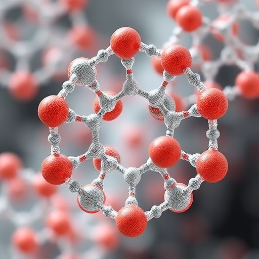
At the core of this leap forward is a sophisticated measurement technique known as multi-slice electron ptychography (MEP). This method entails scanning a nanometer-scale electron probe across the material’s surface and collecting detailed diffraction patterns at overlapping intervals. The resulting data sets contain rich, yet previously inaccessible information, which, when processed via advanced algorithms, reconstruct the full three-dimensional electron wave function and atomic structure of the sample with unprecedented clarity. This ability to ‘peer’ deep within the material’s atomic lattice represents a landmark advance in nanoscopic imaging.
James LeBeau, the Kyocera Professor of Materials Science and Engineering at MIT and the study’s lead corresponding author, emphasized the transformative nature of this insight. “Our ability to directly observe the atomic form allows us to validate and refine predictive models with much higher fidelity,” he explains. “In materials science, ensuring that your computational models align with reality is crucial. Until now, we have been largely reliant on indirect evidence and assumptions that couldn’t be verified experimentally.”
One of the most striking revelations from this work lies in the unexpected role of chemical disorder within the material. Michael Xu and Menglin Zhu, co-first authors and MIT postdoctoral researchers, uncover that the distribution and interplay of different atomic species disrupt previously held models. Classical simulations, which often depicted regions of randomly oriented polarization, overlooked the nuanced correlations between chemistry and electric polarization states. Integrating empirical data from MEP compelled the team to rethink and retool simulation parameters, producing models that better predict actual material behavior.
The material under scrutiny is a compound of lead magnesium niobate-lead titanate, an alloy prized for its application in sensors, defense actuators, and precision medicine devices. Historically, the material’s nanoregions—domains characterized by electric polarization—were too small and complex to resolve fully. The advanced resolution afforded by MEP unveiled a hierarchical mosaic of chemical and polar configurations, extending from atomic scales up to mesoscopic regimes. These findings challenge prior assumptions regarding the size and correlation of polar nanoregions, offering new perspectives on how atomic interactions govern macroscopic functions.
From a methodological standpoint, the technique’s iterative approach in handling diffraction data is intellectually captivating. By intentionally moving the electron beam in overlapping sectors and capturing the resulting complex wave interactions, MEP employs computational reconstruction methods to generate volumetric electron density maps. This contrasts with conventional electron microscopy, which typically yields two-dimensional projections. The additional dimension is pivotal for understanding intricate charge distributions and their spatial relationships, which ultimately dictate the performance of ferroelectric materials.
This work is not merely an imaging achievement; it forms a crucial bridge between experimental visualization and theoretical frameworks such as molecular dynamics simulations. As Xu elaborates, “Connecting three-dimensional polar structures extracted from real specimens with dynamic simulations unveils how individual atoms’ charge states influence collective polarization phenomena, something that models alone previously could not resolve.” Such breakthroughs empower researchers to tailor material properties at the atomic level, unlocking pathways for engineered functionalities.
Beyond relaxor ferroelectrics, the implications of harnessing MEP for disordered and complex materials are profound. The technique’s capacity to elucidate atomistic heterogeneity and correlate it with emergent electronic behaviors could redefine research in semiconductors, metal alloys, and even quantum materials. Zhu notes that this new toolset opens vistas for developing devices with enhanced memory storage, sensitivity, and energy efficiency—capabilities urgently sought in the era of AI and advanced computing.
Underlying this progress is the recognition that computational predictions are only as reliable as the empirical data and validation methods informing them. “Without accurate verification, even the most intricate models can mislead progress,” LeBeau warns. “Multi-slice electron ptychography provides a pivotal feedback loop between theory and reality, ensuring our designs are grounded in the true atomic landscape.” Such integration promises to accelerate the deployment of next-generation materials tailored with atomic precision.
The research received generous support from renowned agencies, including the U.S. Army Research Laboratory, the U.S. Office of Naval Research, the U.S. Department of War, and notable scholarships such as the National Science Graduate Fellowship. Leveraging state-of-the-art MIT.nano facilities enabled the team to deploy this cutting-edge experimental setup, underscoring the synergy of institutional support and pioneering research.
Looking forward, the team envisions a future where electron ptychography transcends current boundaries, offering a standardized approach for direct 3D atomic mapping in a variety of advanced materials. Such technological progress aligns with the expanding complexity in materials design, where machine learning and computational advances demand direct verification at the atomic scale. This marriage of experimental prowess and computational intelligence is poised to drive innovation across electronics, sensing systems, and energy conversion technologies.
Ultimately, this groundbreaking visualization of relaxor ferroelectrics marks a paradigm shift, highlighting the indispensable role of high-fidelity imaging in unraveling the atomic mysteries of complex materials. The insights gleaned pave the way for smarter, more predictive materials engineering and promise to accelerate innovation cycles in critical technological domains worldwide.
Subject of Research: Relaxor ferroelectrics’ three-dimensional atomic structure characterization through multi-slice electron ptychography.
Article Title: Bridging experiment and theory of relaxor ferroelectrics with multislice electron ptychography
News Publication Date: 30-Apr-2026
Web References: http://dx.doi.org/10.1126/science.ads6023
Image Credits: Courtesy of James LeBeau et al
Keywords
Materials science, Material properties, Materials engineering, Materials, Electronics, Sensors, Ferroelectricity, Technology, Nanotechnology, Semiconductors, Electrical conductors, Physics
Tags: 3D atomic blueprint of materialsadvanced diffraction pattern analysisatomic lattice visualizationcomputational materials designelectro-mechanical properties of materialselectron ptychography techniqueMIT materials science researchmulti-slice electron ptychographynanoscale electron probe scanningnanoscopic imaging breakthroughsnext-generation sensing technologiesrelaxor ferroelectrics atomic structure


