
Credit: University of Texas at Dallas
For several years, a team of researchers at The University of Texas at Dallas has investigated various materials in search of those whose electrical properties might make them suitable for small, energy-efficient transistors to power next-generation electronic devices.
They recently found one such material, but it was nothing anyone expected.
In an article published online March 10 in the journal Advanced Materials, Dr. Moon Kim and his colleagues describe a material that, when heated to about 450 degrees Celsius, transforms from an atomically thin, two-dimensional sheet into an array of one-dimensional nanowires, each just a few atoms wide.
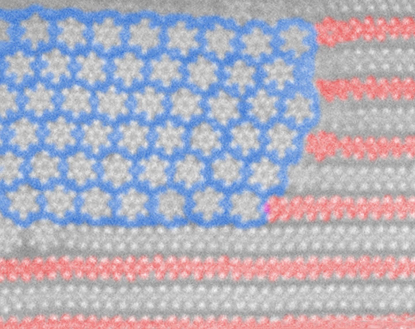
An image caught in mid-transformation looks like a tiny United States flag, and with false colors added, is arguably the world's smallest image of Old Glory, Kim said.
"The phase transition we observed, this new structure, was not predicted by theory," said Kim, the Louis Beecherl Jr. Distinguished Professor of materials science and engineering at UT Dallas.
Because the nanowires are semiconductors, they might be used as switching devices, just as silicon is used in today's transistors to turn electric current on and off in electronic devices.
"These nanowires are about 10 times smaller than the smallest silicon wires, and, if used in future technology, would result in powerful energy-efficient devices," Kim said. The lead authors of the study are Hui Zhu and Qingxiao Wang, graduate students in materials science and engineering in the Erik Jonsson School of Engineering and Computer Science.
Just a Phase?
When certain materials are subjected to changes in external conditions, such as temperature or pressure, they can undergo a phase transition. A familiar example is when liquid water is cooled to form a solid (ice), or heated to form a gas (steam).
For many materials, however, a phase transition means something a little different. As external temperature and pressure change, these materials' atoms rearrange and redistribute to make a material with a different structure and composition. These changes can affect the new material's properties, such as how electrons move through it. For scientists interested in new applications for materials, understanding such transitions is paramount.
In most cases, a type of graphic called a phase diagram helps researchers predict structural and property changes in a material when it undergoes a phase transition.
But nothing predicted what Kim's team observed as it conducted experiments on a material called molybdenum ditelluride.
Nanoflags and Nanoflowers
Using a transmission electron microscope, the researchers started with atomically thin, two-dimensional sheets of molybdenum ditelluride, a material made up of one layer of molybdenum atoms and two layers of tellurium atoms. The material belongs to a class called transition metal dichalcogenides (TMDs), which show promise in replacing silicon in transistors.
"We wanted to understand the thermal stability of this particular material," Kim said. "We thought it was a good candidate for next-generation nanoelectronics. Out of curiosity, we set out to see whether it would be stable above room temperature."
When they increased the temperature to above 450 degrees Celsius, two things happened.
"First, we saw a new pattern begin to emerge that was aesthetically pleasing to the eye," Kim said. Across the surface of the sample, the repeating rows, or stripes, of molybdenum ditelluride layers began to transform into shapes that looked like tiny six-pointed stars, or flowers with six petals.
The material was transitioning into hexa-molybdenum hexa-telluride, a one-dimensional wire-like structure. The cross section of the new material is a structure consisting of six central atoms of molybdenum surrounded by six atoms of tellurium.
As the phase transition progressed, part of the sample was still "stripes" and part had become "stars." The team thought the pattern looked like a United States flag. They made a false-color version with a blue field behind the stars and half of the stripes colored red, to make a "nanoflag."
Not in the textbooks
"Then, when we examined the material more closely, we found that the transition we were seeing from 'stripes' to 'stars' was not in any of the phase diagrams," Kim said. "Normally, when you heat up particular materials, you expect to see a different kind of material emerge as predicted by a phase diagram. But in this case, something unusual happened — it formed a whole new phase."
Each individual nanowire is a semiconductor, which means that electric current moving through the wire can be switched on and off, Kim said. When many of the individual nanowires are grouped together in bulk they behave more like a metal, which easily conducts current.
"We would want to use the nanowires one at a time because we are pushing the size of a transistor as small as possible," Kim said. "Currently, the smallest transistor size is about 10 times larger than our nanowire. Each of ours is smaller than 1 nanometer in diameter, which is essentially an atomic-scale wire.
"Before we can put this discovery to use and make an actual device, we have many more studies to do, including determining how to separate out the individual nanowires, and overcoming technical challenges to manufacturing and mass production," Kim said. "But this is a start."
###
Other authors of the study are: graduate student Chenxi Zhang, research scientist Rafik Addou, Dr. Kyeongjae "K.J." Cho, professor of materials science and engineering, and Dr. Robert Wallace, professor of materials science and engineering and holder of the Erik Jonsson Distinguished Chair.
The research was funded in part by the South West Academy of Nanoelectronics, which is supported by the Semiconductor Research Corporation (SRC) and the National Institute of Standards and Technology; and the Center for Low Energy Systems Technology, one of the six STARnet centers that are sponsored by the Defense Advanced Research Projects Agency and the SRC.
Media Contact
Amanda Siegfried
[email protected]
903-366-1994
@ut_dallas
http://www.utdallas.edu
############
Story Source: Materials provided by Scienmag

