
Credit: Frank Ceballos | University of Kansas
LAWRENCE – Common sense might dictate that for an object to move from one point to another, it must go through all the points on the path.
"Imagine someone driving from Kansas City to Topeka on I-70 — it's safe to say that he must be in Lawrence at some point during the trip," said Hui Zhao, associate professor of physics & astronomy at the University of Kansas. "Or in basketball, when KU's Josh Jackson receives an alley-oop pass from Frank Mason III and dunks the ball from above to below the rim, the ball must be in the hoop at some point in time."
Not so for electrons in the quantum world, which don't follow such common-sense rules for the most part.
"Electrons can show up on the first floor, then the third floor, without ever having been on the second floor," Zhao said.
Zhao, along with KU physics graduate student Frank Ceballos and Self Graduate Fellow Samuel Lane, has just observed the counterintuitive motion of electrons during experiments in KU's Ultrafast Laser Lab.
"In a sample made of three atomic layers, electrons in the top layer move to the bottom layer, without ever being spotted in the middle layer," said the KU researcher.
Because this sort of "quantum" transport is very efficient, Zhao said it can play a key role in a new type of manmade material called "van der Waals materials" that could be used someday in solar cells and electronics.
Their findings were just published in Nano Letters, a premier journal on nanoscience and nanotechnology.
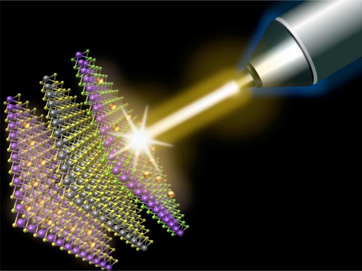
The KU research team fabricated the sample by using the "Scotch tape" method, where single-molecule layers are lifted from a crystal with tape, then verified under an optical microscope. The sample contains layers of MoS2, WS2 and MoSe2 — each layer thinner than one nanometer. All three are semiconductor materials and respond to light with different colors. Based on that, the KU researchers used a laser pulse of 100 femtosecond duration to liberate some of the electrons in the top MoSe2 layer so they could move freely.
"The color of the laser pulse was chosen so that only electrons in the top layer can be liberated," Zhao said. "We then used another laser pulse with the 'right' color for the bottom MoS2 layer to detect the appearance of these electrons in that layer. The second pulse was purposely arranged to arrive at the sample after the first pulse by about 1 picosecond, by letting it travel a distance 0.3 mm longer than the first."
The team found electrons move from the top to the bottom layer in about one picosecond on average.
"If electrons were things that followed 'common sense,' like so-called classical particles, they'd be in the middle layer at some point during this one picosecond," Zhao said.
The researchers used a third pulse with another color to monitor the middle layer and found no electrons. The experimental discovery of the counterintuitive transport of electrons in the stack of atomic layers was further confirmed by simulations performed by theorists Ming-Gang Ju and Xiao Cheng Zeng at the University of Nebraska-Lincoln, who co-authored the paper. According to Zhao, the verification of quantum transport of electrons between atomic layers connected by van der Waals force is encouraging news for researchers developing new materials.
"The Stone Age, Bronze Age and Iron Age — materials have been the defining element of human history," he said. "The modern information-technology age is largely based on silicon, which is a result of many decades of material research focused on finding new materials and developing better techniques to make them with high quality and low cost."
Zhao said in recent decades researchers have learned to tune properties of materials by changing their size and shape on a nanometer scale. A new form of nanomaterials, known as two-dimensional materials, was discovered about a decade ago. "They are formed by single layers of atoms or molecules," he said. "The most well-known example is graphene, a single layer of carbon atoms. So far, about 100 types of two-dimensional materials have been discovered, such as the three used in this study. Because these atomic layers can be stacked by using van der Waals force, they opened up an entirely new route to make new functional materials."
The researcher said his team's work focused on a key requirement for such materials to be ideal for electronic and optical applications: Electrons must be able to move between these atomic layers efficiently.
"This study showed electrons can transfer between these layers in a quantum fashion, just like in other conductors and semiconductors," he said.
###
The National Science Foundation funded this research. Lane was supported by the Self Graduate Fellowship.
Media Contact
Brendan M. Lynch
[email protected]
785-864-8855
@KUNews
http://www.news.ku.edu
############
Story Source: Materials provided by Scienmag


