
In the ever-evolving landscape of semiconductor technology, the demand for more compact, faster, and more efficient electronic devices propels continuous innovation in materials characterization and device analysis techniques. Silicon (Si) large-scale integration (LSI) manufacturing, foundational to modern electronics, grapples with challenges associated with the miniaturization and three-dimensional structuring of components. Among these challenges is the pressing need for reliable, rapid, and non-invasive evaluation methods capable of probing the internal characteristics of silicon wafers, crucially the depth profile of buried PN junctions, without physical contact or destruction of the sample.
Addressing this intricate challenge, a groundbreaking study recently published in Light: Science & Applications details a novel, non-contact terahertz (THz) emission spectroscopy technique that enables nanometer-scale resolution measurement of PN junction depth in silicon wafers. This method, pioneered through an international collaboration led by Professor Masayoshi Tonouchi at Okayama University alongside researchers from Rice University and Samsung Electronics, introduces a paradigm shift in semiconductor wafer inspection technology. The approach harnesses the unique properties of ultrafast laser pulses and the resulting THz electromagnetic waves emitted from photogenerated carriers at the PN junction interface.
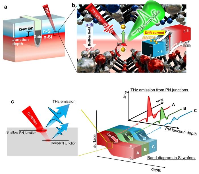
Fundamentally, this technique exploits the generation and detection of THz waves initiated by femtosecond laser illumination of the semiconductor junction. When a buried PN junction in the silicon wafer is irradiated with an ultrashort femtosecond laser pulse, photocarrier generation occurs selectively at the depletion region. These photocarriers—electrons and holes—are rapidly accelerated in opposite directions by the built-in electric field intrinsic to the PN junction. The transient drift current produced by this separation of charge carriers induces the emission of THz electromagnetic waves, which serve as a direct probe of the electronic and structural properties at the junction.
.adsslot_k0eNOg5DBT{width:728px !important;height:90px !important;}
@media(max-width:1199px){ .adsslot_k0eNOg5DBT{width:468px !important;height:60px !important;}
}
@media(max-width:767px){ .adsslot_k0eNOg5DBT{width:320px !important;height:50px !important;}
}
ADVERTISEMENT
The crucial insight realized by the research team is that the amplitude and spectral characteristics of the emitted THz waves are highly sensitive to the depth at which the PN junction resides within the wafer. This sensitivity arises because the photocarrier density and ensuing ultrafast carrier dynamics vary with the junction depth, altering the resultant THz signal. By constructing a detailed physical model correlating THz emission profiles to junction depth, the researchers demonstrated the ability to non-destructively and precisely map the PN junction depth with nanoscale accuracy.
A key technical hurdle overcome in this work relates to the optical penetration depth of common femtosecond laser wavelengths in silicon. Typically, lasers operating near 800 nm wavelength—commonly used in THz emission setups—penetrate too deeply into silicon, on the order of tens of micrometers, obscuring the photoexcitation of shallow PN junctions buried mere nanometers below the surface. As Dr. Fumikazu Murakami, a leading young scientist on the team, explains, tuning the excitation wavelength closer to the half-wavelength condition compatible with the junction depth enables selective excitation of shallow junctions. This carefully optimized wavelength selection ensures that photocarrier generation occurs specifically at the junction interface, permitting accurate depth-resolved measurements.
This innovative spectroscopic methodology not only advances the fundamental understanding of ultrafast photocarrier transport mechanisms in semiconductor junctions but also opens transformative possibilities for the semiconductor manufacturing industry. The capability to perform rapid, non-contact, and non-destructive assessment of internal electric fields, carrier transport behavior, and junction depth is poised to enhance quality control, device reliability, and yield in LSI production lines. These enhancements become critical as device architectures adopt more complex three-dimensional morphologies and continue to scale down in size.
Moreover, the developed technique represents a significant leap beyond conventional semiconductor metrology tools, which often require destructive sample preparation, laborious contact measurements, or are limited by spatial resolution constraints. By providing a direct optical window into the junction dynamics and geometry, terahertz emission spectroscopy as implemented in this study affords unparalleled insight into buried semiconductor structures. This technology fulfills the rising industrial demand for advanced wafer testing solutions that can be seamlessly integrated into manufacturing without compromising device integrity.
Professor Tonouchi emphasizes the intuitive nature of the depth estimation process, underpinned by a simplified but effective model of ultrafast carrier motion and THz wave generation at the PN junction. The ability to translate complex photocarrier phenomena into actionable metrological data marks a milestone in semiconductor inspection capabilities. Researchers anticipate that ongoing refinements, including optimization of excitation pulse characteristics and detection schemes, will further enhance spatial resolution and sensitivity for a variety of semiconductor materials and device configurations.
Looking to the future, this breakthrough is expected to drive collaborative innovations across academia and industry, stimulating the development of next-generation semiconductor devices with unprecedented performance and integration density. The versatility of the THz emission spectroscopy platform opens pathways to investigating other deeply embedded structures within wafers, such as buried contacts, defects, and multi-layered heterojunctions. Its nondestructive nature also aligns well with sustainability goals by minimizing waste and material consumption during device fabrication and testing.
Furthermore, this research underscores the interdisciplinary synergy between ultrafast optics, solid-state physics, and semiconductor engineering. The fusion of precise laser technology with comprehensive semiconductor device knowledge enables the probing of ultrafast transient phenomena that were previously elusive to conventional diagnostic techniques. Such integration of expertise is instrumental in overcoming contemporary challenges posed by shrinking device dimensions and increasing functional complexity.
In conclusion, the demonstration of non-contact, nanometer-scale measurement of PN junction depth buried in silicon wafers using terahertz emission spectroscopy heralds a new era in semiconductor metrology. This method combines ultrafast photocarrier excitation, THz wave generation, and sophisticated optical detection to yield rapid, accurate, and non-destructive characterization of critical device parameters. It sets a benchmark for future wafer inspection technologies, contributing to the advancement of electronic device manufacturing and quality assurance at the nanoscale. As semiconductor devices become even more integral to technological innovation, such transformative analysis techniques will be essential to sustain progress and maintain the pace of miniaturization.
Subject of Research: Non-contact, nanometer-scale measurement of PN junction depth in silicon wafers using terahertz emission spectroscopy
Article Title: Non-contact and nanometer-scale measurement of PN junction depth buried in Si wafers using terahertz emission spectroscopy
Web References:
DOI: 10.1038/s41377-025-01911-0
Image Credits: Fumikazu Murakami, Shinji Ueyama et al.
Keywords
Terahertz emission spectroscopy, PN junction depth, silicon wafers, non-destructive evaluation, femtosecond laser, photocarrier transport, semiconductor metrology, ultrafast optics, nanometer-scale resolution, non-contact measurement, semiconductor manufacturing, buried junction characterization
Tags: advanced semiconductor inspection methodsburied junction profiling in siliconinternational collaboration in semiconductor researchLSI manufacturing challengesnanometer-scale semiconductor analysisnon-contact terahertz spectroscopynon-invasive material evaluationPN junction depth measurementsemiconductor technology innovationssilicon wafer characterizationterahertz wave generation in semiconductorsultrafast laser techniques in electronics


