Conventional microscopes irradiate a sample, usually with light or electrons. Any reflected or scattered radiation can be used to build a detailed image and obtain characteristic information about a material’s surface. This is called an active measurement, but it isn’t the only technique that can be used. Researchers from Japan have been developing a new form of microscopy that can probe details in an object’s surface, like the distribution of a material’s lattice and electron temperatures, with nanoscale precision.
Credit: Institute of Industrial Science, The University of Tokyo
Conventional microscopes irradiate a sample, usually with light or electrons. Any reflected or scattered radiation can be used to build a detailed image and obtain characteristic information about a material’s surface. This is called an active measurement, but it isn’t the only technique that can be used. Researchers from Japan have been developing a new form of microscopy that can probe details in an object’s surface, like the distribution of a material’s lattice and electron temperatures, with nanoscale precision.
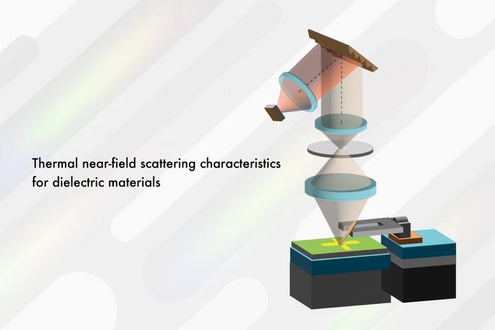
Evanescent waves are short-lived electromagnetic waves that do not transport energy, a little like ripples on a material’s surface. They can be created when light interacts with the surface, but can also be generated thermally. All matter contains energy and emits heat, and localized heat fluctuations in a material can briefly create strong evanescent waves. The key to this powerful new form of microscopy, developed by researchers from the Institute of Industrial Science, The University of Tokyo, is in passively detecting these waves.
“Scanning near-field optical microscopy, using scattered electromagnetic radiation, is one of the most commonly used techniques for examining material properties at the nanoscale level,” explains lead author Ryoko Sakuma. Using thermal infrared wavelengths, the team can observe details that are undetectable by other means. “Our new technique uses passive detection of the radiation emitted by the object itself, so the surface doesn’t need any illumination.”
Using their prototype instrument, the researchers examined thermally excited evanescent waves generated in two dielectric materials: aluminum nitride and gallium nitride. The weak scattering, which was unpredicted, can be seen in an absorption band called the Reststrahlen band. This is the first time such a phenomenon was observed without light exposure. Most significantly, their spectroscopic analysis showed that only the polariton waves (i.e., waves caused by surface phonon resonance) exist in the Reststrahlen band, despite theoretical predictions that these polariton waves would be accompanied by a large amount of thermal fluctuation. These results help us to understand thermally excited evanescent waves in this band and lay the groundwork for an improved passive detection model to identify dielectric materials.
The team is keen to further develop this technology. “Our instrument is the only one in the world capable of observing nanoscale temperature distributions on surfaces using terahertz wavelengths.” explains senior author, Yusuke Kajihara. The terahertz wavelength range starts in the mid-infrared, from around 10 µm, extending up to 1 mm. As a prototype, improving the way the instrument functions is currently a major goal. “This microscope technology is completely new, so we’re still learning specifically how and where it can be applied,” Kajihara adds.
The team intends to further improve their prototype instrument and refine how the technique works. Their next step is to develop an improved detection model. The goal is greater versatility, resulting in a new and powerful non-destructive characterization technique, allowing highly localized analysis of a material’s surface dynamics.
###
The article, “Thermal near-field scattering characteristics for dielectric materials,” was published in Scientific Reports at DOI: 10.1038/s41598-023-44920-y
About Institute of Industrial Science, The University of Tokyo
The Institute of Industrial Science, The University of Tokyo (UTokyo-IIS) is one of the largest university-attached research institutes in Japan. UTokyo-IIS is comprised of over 120 research laboratories—each headed by a faculty member—and has over 1,200 members (approximately 400 staff and 800 students) actively engaged in education and research. Its activities cover almost all areas of engineering. Since its foundation in 1949, UTokyo-IIS has worked to bridge the huge gaps that exist between academic disciplines and real-world applications.
Journal
Scientific Reports
DOI
10.1038/s41598-023-44920-y
Article Publication Date
16-Oct-2023


