Scientists achieve remarkable precision in measuring atomic displacements by combining electron microscopy with a technique borrowed from data science

Credit: Kohei Aso from JAIST.
Ishikawa, Japan – Sometimes, a material’s property, such as magnetism and catalysis, can change drastically owing to nothing more than minute changes in the separation between its atoms, commonly referred to as “local strains” in the parlance of materials science. A precise measurement of such local strains is, therefore, important to materials scientists.
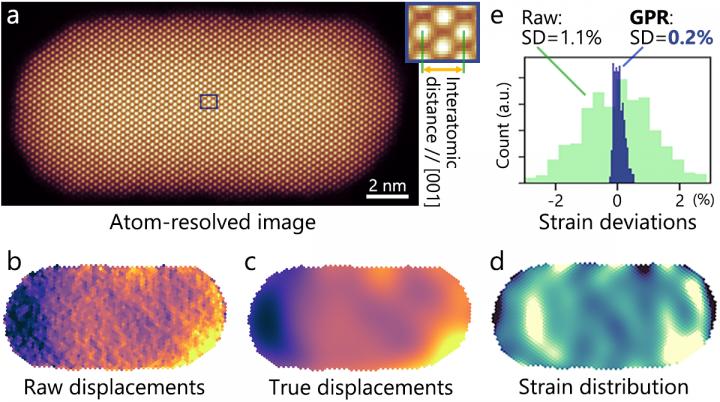
One powerful technique employed for this purpose is “high-angle annular dark-field imaging” (HAADF), an approach within scanning transmission electron microscopy (a technique for mapping the position of atoms within materials), that produces images with bright spots that theoretically coincide with atomic positions. However, in practice, HAADF images are often distorted due to mechanical and electrical noise in the apparatus, limiting the smallest measurable local strains to slightly over 1%.
Now, a team of scientists led by Assistant Professor Kohei Aso from Japan Advanced Institute of Science and Technology (JAIST), Japan, have leveraged a method from the field of data science to measure strain distribution in materials more accurately, improving the precision of HAADF imaging. This study, published in ACS Nano, was carried out in collaboration with JAIST Professor Yoshifumi Oshima, then graduate student Jens Maebe, post-doctoral fellow Xuan Quy Tran, Assistant Professor Tomokazu Yamamoto, and Professor Syo Matsumura from Kyushu University, Japan.
The team combined HAADF imaging with Gaussian process regression (GPR), a data processing technique commonly used in machine learning and fields such as economics and geology. In a Gaussian process, the true state of data (in this case, atomic positions or displacement) is assumed to be represented by a smooth function, and random noise is added to this ‘true state’ when data is observed. By reversing this process through GPR, one can more accurately estimate the true positions of the atoms, and thus calculate local strains with higher precision. Specifically, the proposed method enabled the team to measure strain with a precision of 0.2%.
The team demonstrated the potential of their approach by measuring local strains in gold nanostructures and comparing tensile strains in a gold nanosphere with those in gold nanorods (essentially cylinders with hemispherical caps) of different lengths. These comparisons revealed that strain distributions in gold nanoparticles varied depending on their shape, with nanorods exhibiting a tensile strain of about 0.5% near the region where curvature abruptly changes. Dr. Aso explains the motivation behind these specific experiments: “It is known that spherical gold nanoparticles are subjected to uniform stress over their entire surface, and this stress is proportional to surface tension. Thus, uniform compressive strain occurs in the direction perpendicular to the surface. In contrast, in gold nanorods, the stress applied to the surface becomes non-uniform, and scientists have theorized that tensile strain should occur in certain places. However, this had not been proven experimentally, until now.”
With these findings, the team is thrilled about the future prospects of their strain measurement strategy. “Our technique will provide detailed information on the atomic world, which is necessary for the development of innovative materials and devices with both high performance and small size. This could be useful for the development of devices and sensors employing nanoscale materials and structures. Moreover, the method requires no expensive modifications or complicated procedures and can be readily adopted, “ says Dr. Aso.
One thing’s for sure: we can now understand and manipulate the atomic world even better!
###
Reference
Title of original paper: “Subpercent Local Strains due to the Shapes of Gold Nanorods Revealed by Data-Driven Analysis”
Journal: ACS Nano
DOI: 10.1021/acsnano.1c03413
About Japan Advanced Institute of Science and Technology, Japan
Founded in 1990 in Ishikawa prefecture, the Japan Advanced Institute of Science and Technology (JAIST) was the first independent national graduate school in Japan. Now, after 30 years of steady progress, JAIST has become one of Japan’s top-ranking universities. JAIST counts with multiple satellite campuses and strives to foster capable leaders with a state-of-the-art education system where diversity is key; about 40% of its alumni are international students. The university has a unique style of graduate education based on a carefully designed coursework-oriented curriculum to ensure that its students have a solid foundation on which to carry out cutting-edge research. JAIST also works closely both with local and overseas communities by promoting industry-academia collaborative research.
About Assistant Professor Kohei Aso from Japan Advanced Institute of Science and Technology, Japan
Dr. Kohei Aso joined JAIST as an Assistant Professor at the School of Materials Science in 2020. He obtained a PhD in Engineering from Kyushu University, Japan. His research interests lie at the intersection between statistical science and nanomaterials; he specializes in electron microscopy, data science, and materials research. He has published seven research papers, some of which were selected as Editor’s Pick in the prestigious Microscopy journal. He is also a member of both The Japan Society of Applied Physics and The Japanese Society of Microscopy.
Funding information
This study was partly financially supported by a Grant-in-Aid for Scientific Research B (No. 25289221 and No. 18H01830) from Japan Society for the Promotion of Science, the ACCEL program (JPMJAC1501), Japan Science and Technology Agency (JST), and the Education and Research Support Program on Mathematics and Data Science 2017 from Kyushu University.
Media Contact
Kohei Aso
[email protected]
Related Journal Article
http://dx.


