• HOME
  • NEWS
  • EXPLORE
    • CAREER
      • Companies
      • Jobs
    • EVENTS
    • iGEM
      • News
      • Team
    • PHOTOS
    • VIDEO
    • WIKI
  • BLOG
  • COMMUNITY
    • FACEBOOK
    • INSTAGRAM
    • TWITTER
Sunday, June 28, 2026
BIOENGINEER.ORG
No Result
View All Result
  • Login
  • HOME
  • NEWS
  • EXPLORE
    • CAREER
      • Companies
      • Jobs
        • Lecturer
        • PhD Studentship
        • Postdoc
        • Research Assistant
    • EVENTS
    • iGEM
      • News
      • Team
    • PHOTOS
    • VIDEO
    • WIKI
  • BLOG
  • COMMUNITY
    • FACEBOOK
    • INSTAGRAM
    • TWITTER
No Result
View All Result
Bioengineer.org
No Result
View All Result
Home NEWS Science News Chemistry

Deciphering the secrets of printed electronics

Bioengineer by Bioengineer
March 29, 2021
in Chemistry
Reading Time: 2 mins read
0
IMAGE
Share on FacebookShare on TwitterShare on LinkedinShare on RedditShare on Telegram

We live in a world where we want our electronics to be flexible, bendable and stretchable apart from being intelligent. Printed electronics technology has emerged as the main route to enable this vision.

IMAGE

Credit: Shweta Agarwala

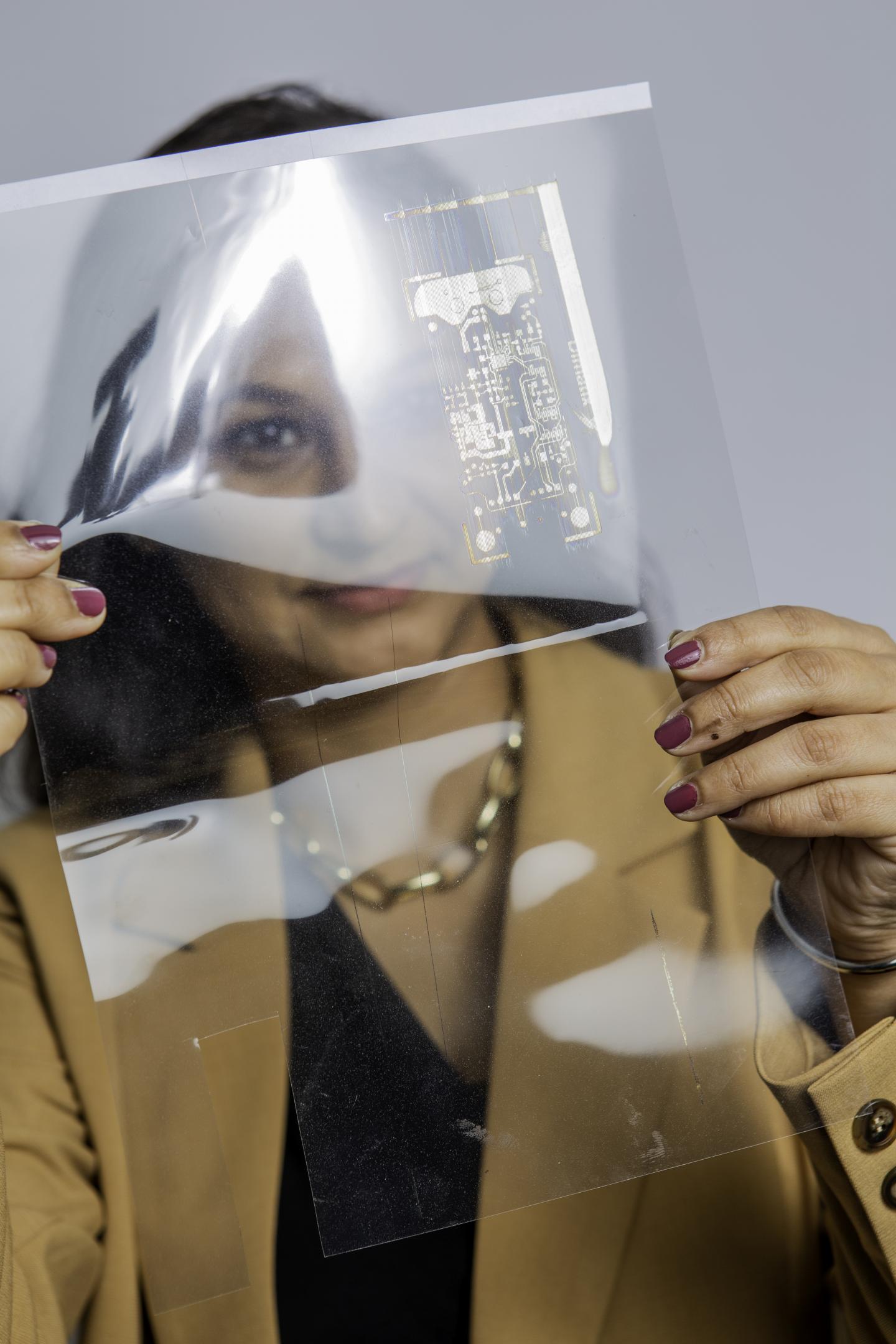
Next-gen electronics is envisioned to be non-rigid, component-free, flexible, bendable, and easily integrable with different objects.

Direct-write printing techniques provide unique opportunity to enable this vision through use of nanomaterial so-called functional inks, that can be tailored to add desired functionalities on various flexible substrates, such as textiles or plastic.

The technology, known as Printed Electronics (PE), has been known for decades, but has recently gained considerable attention due to innovation in material inks, process technology and design revolution.

To keep the research community abreast with the latest technological advancements in the area of droplet-based PE techniques for next-gen devices, researchers from Aarhus University have now published a comprehensive review of the technology in the prestigious scientific journal Advanced Materials.

“Through this paper, we have tried to fill the existing void in literature by discussing techniques, material inks, ink properties, post processing, substrates and application to provide a complete guide. PE is an industry relevant technology and the gateway to future portable electronics, where advanced printers can print complex circuits on any material,” says Assistant Professor Shweta Agarwala, an expert in PE at the Department of Electrical and Computer Engineering at Aarhus University.

PE is already being used for many different applications today. It is an attractive method to impart electrical functionality on any surface and the major advantage of PE is that it is inexpensive and readily scalable.

“PE offers a wide range of advantages over conventional lithography-based technologies. It provides much more production flexibility, it is cheaper and far simpler. More importantly, it opens up a plethora of new possibilities to print flexible electrical circuits directly onto a wide range of substrates such as plastics, papers, clothes, and quite literally any other planar and non-planar surfaces. The research area is moving forwards fast, and this publication provides an overview of how far we have progressed today,” says Hamed Abdolmaleki, a PhD student and first author of the paper.

Even though PE is being used in more and more industries, and is considered very important in the electronics of the future, the technology is still in its infancy.

For Shweta Agarwala, the sustainability aspect is very important for the future perspectives of electronics and PE technology:

“PE is the way towards biodegradable electronics, and with this technology, we can address the huge societal problem that electronics already present, and which will only get more pressing in the future. The world is not only suffering from a huge amount of plastic pollution; it is also burdened by enormous pollution from electronics in all the devices we discard rapidly. In the review article, we have also discussed the emerging field of biodegradable substrates that will have huge environmental impact,” she adds.

###

Media Contact
Assistant Professor Shweta Agarwala
[email protected]

Related Journal Article

http://dx.doi.org/10.1002/adma.202006792

Tags: Chemistry/Physics/Materials SciencesComputer ScienceElectrical Engineering/ElectronicsHardwareMaterialsResearch/DevelopmentSuperconductors/SemiconductorsTechnology TransferTechnology/Engineering/Computer Science
Share13Tweet8Share2ShareShareShare2

Related Posts

AI and Physics Collaborate to Design Advanced Hydrogen Storage Materials

June 25, 2026

International Team Including Dresden Scientists Develops Novel Designer Proteins for Advanced Study of Living Tissue

June 25, 2026

New Study Uncovers Key Factors Driving Water Chemistry in Nanoscale Environments

June 25, 2026

Plasma Technology Extends Catalyst Lifespan in Hydrogen Production

June 24, 2026
Please login to join discussion

POPULAR NEWS

  • Saying Goodbye to PGY-6: Pediatric Fellowship Realities

    103 shares
    Share 41 Tweet 26
  • Multi-Hospital Study Reveals Long Covid Burden Is Twice as High as Current Estimates

    92 shares
    Share 36 Tweet 23
  • Detection of EDCs in Breast Milk and Infant Urine Up to Six Months Highlights Early Exposure Risks

    77 shares
    Share 31 Tweet 19
  • New Drug Candidate Developed at McMaster Shows Potential for Treating Brain Cancer

    58 shares
    Share 23 Tweet 15

About

We bring you the latest biotechnology news from best research centers and universities around the world. Check our website.

Follow us

Recent News

Tracking Lanthanide-Labeled Microplastics in Plants

POSTECH Researchers Slash Cost of Reconstituted Cell-Free Systems by 95%

AI and Physics Collaborate to Design Advanced Hydrogen Storage Materials

Subscribe to Blog via Email

Success! An email was just sent to confirm your subscription. Please find the email now and click 'Confirm' to start subscribing.

Join 82 other subscribers
  • Contact Us

Bioengineer.org © Copyright 2023 All Rights Reserved.

Welcome Back!

Login to your account below

Forgotten Password?

Retrieve your password

Please enter your username or email address to reset your password.

Log In
No Result
View All Result
  • Homepages
    • Home Page 1
    • Home Page 2
  • News
  • National
  • Business
  • Health
  • Lifestyle
  • Science

Bioengineer.org © Copyright 2023 All Rights Reserved.