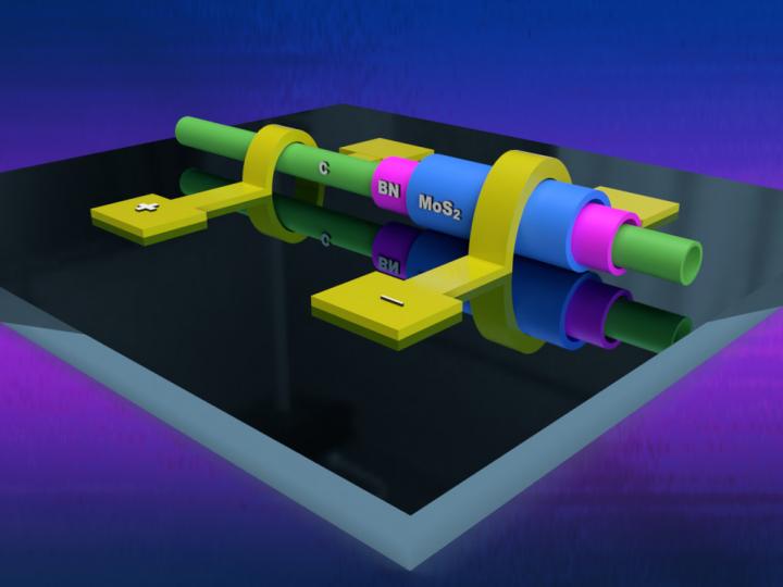
Credit: ELIZABETH FLORES-GOMEZ MURRAY/ PENN STATE
The recent synthesis of one-dimensional van der Waals heterostructures, a type of heterostructure made by layering two-dimensional materials that are one atom thick, may lead to new, miniaturized electronics that are currently not possible, according to a team of Penn State and University of Tokyo researchers.
Engineers commonly produce heterostructures to achieve new device properties that are not available in a single material. A van der Waals heterostructure is one made of 2D materials that are stacked directly on top of each other like Lego-blocks or a sandwich. The van der Waals force, which is an attractive force between uncharged molecules or atoms, holds the materials together.
According to Slava V. Rotkin, Penn State Frontier Professor of Engineering Science and Mechanics, the one-dimensional van der Waals heterostructure produced by the researchers is different from the van der Waals heterostructures engineers have produced thus far.
“It looks like a stack of 2D-layered materials that are rolled up in a perfect cylinder,” Rotkin said. “In other words, if you roll up a sandwich, you keep all the good stuff in it where it should be and not moving around, but in this case you also make it a thin cylinder, very compact like a hot-dog or a long sushi roll. In this way, the 2D-materials still contact each other in a desired vertical heterostructure sequence while one needs not to worry about their lateral edges, all rolled up, which is a big deal for making super-small devices.”
The team’s research, published in ACS Nano, suggests that all 2D materials could be rolled into these one-dimensional heterostructure cylinders, known as hetero-nanotubes. The University of Tokyo researchers recently fabricated electrodes on a hetero-nanotube and demonstrated that it can work as an extremely small diode with high performance despite its size.
“Diodes are a major type of device used in optoelectronics — they are in the core of photodetectors, solar cells, light emitting devices, etc.,” Rotkin said. “In electronics, diodes are used in several specialized circuits; although the main element of electronics is a transistor, two diodes, connected back-to-back, may serve as a switch, too.”
This opens a potential new class of materials for miniaturized electronics.
“It brings device technology of 2D materials to a new level, potentially enabling a new generation of both electronic and optoelectronic devices,” Rotkin said.
Rotkin’s contribution to the project was to solve a particularly challenging task, which was ensuring that they were able to make the one-dimensional van der Waals heterostructure cylinder have all the required material layers.
“Using the sandwich analogy again, we needed to know whether we had a shell of ‘roast beef’ along the entire length of a cylindrical sandwich or if there were regions where we have only ‘bread’ and ‘lettuce’ shells,” Rotkin said. “Absence of a middle insulating layer would mean we failed in device synthesis. My method did explicitly show the middle shells were all there along the entire length of the device.”
In regular, flat van der Waals heterostructures, confirming existence or absence of some layers can be done easily because they are flat and have a large area. This means a researcher can use various type microscopies to collect a lot of signal from the large, flat areas, so they are easily visible. When researchers roll them up, like in the case of a one-dimensional van der Waals heterostructure, it becomes a very thin wire-like cylinder that is hard to characterize because it gives off little signal and becomes practically invisible. In addition, in order to prove the existence of insulating layer in the semiconductor-insulator-semiconductor junction of the diode, one needs to resolve not just the outer shell of the hetero-nanotube but the middle one, which is completely shadowed by the outer shells of a molybdenum sulfide semiconductor.
To solve this, Rotkin used a scattering Scanning Near-field Optical Microscope that is part of the Material Research Institute’s 2D Crystal Consortium, which can “see” the objects of nanoscale size and determine their materials optical properties. He also developed a special method of analysis of the data known as hyperspectral optical imaging with nanometer resolution, which can distinguish different materials and, thus, test the structure of the one-dimensional diode along its entire length.
According to Rotkin, this is the first demonstration of optical resolution of a hexagonal boron nitride (hBN) shell as a part of a hetero-nanotube. Much larger pure hBN nanotubes, consisting of many shells of hBN with no other types of material, were studied in the past with a similar microscope.
“However, imaging of those materials is quite different from what I have done before,” Rotkin said. “The beneficial result is in the demonstration of our ability to measure the optical spectrum from the object, which is an inner shell of a wire that is just two nanometers thick. It’s comparable to the difference between being able to see a wooden log and being able to recognize a graphite stick inside the pencil through the pencil walls.”
Rotkin plans to expand his research to extend hyperspectral imaging to better resolve other materials, such as glass, various 2D materials, and protein tubules and viruses.
“It is a novel technique that will lead to, hopefully, future discoveries happening,” Rotkin said.
###
Along with Rotkin, other authors of the paper include Ya Feng, Henan Li, Taiki Inoue, Shohei Chiashi, Rong Xiang and Shigeo Maruyama, from the University of Tokyo.
The research was funded in part by the Center for Nanoscale Science, which is Penn State’s National Science Foundation Materials Research Science and Engineering Center, and by the Japan Ministry of Education, Culture, Sports, Science and Technology.
Media Contact
A’ndrea Elyse Messer
[email protected]
Related Journal Article
http://dx.


