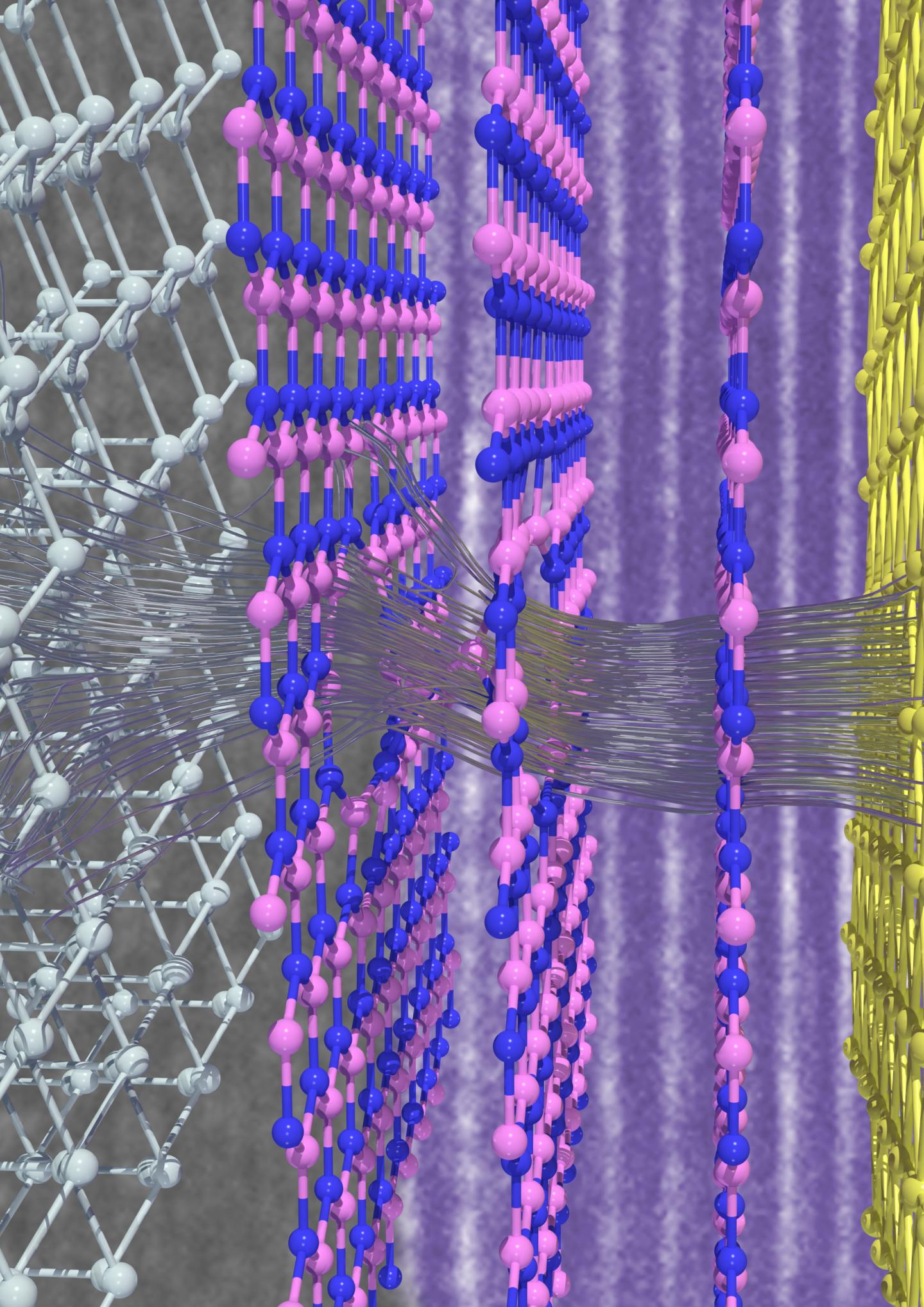
Until now, hexagonal boron nitride was considered the insulator of choice for miniaturized transistors — new investigations by TU Wien (Vienna) show: This may not be the way to go

Credit: TU Wien
For decades, there has been a trend in microelectronics towards ever smaller and more compact transistors. 2D materials such as graphene are seen as a beacon of hope here: they are the thinnest material layers that can possibly exist, consisting of only one or a few atomic layers. Nevertheless, they can conduct electrical currents – conventional silicon technology, on the other hand, no longer works properly if the layers become too thin.
However, such materials are not used in a vacuum; they have to be combined with suitable insulators – in order to seal them off from unwanted environmental influences, and also in order to control the flow of current via the so-called field effect. Until now, hexagonal boron nitride (hBN) has frequently been used for this purpose as it forms an excellent environment for 2D materials. However, studies conducted by TU Wien, in cooperation with ETH Zurich, the Russian Ioffe Institute and researchers from Saudi Arabia and Japan, now show that, contrary to previous assumptions, thin hBN layers are not suitable as insulators for future miniaturised field-effect transistors, as exorbitant leakage currents occur. So if 2D materials are really to revolutionise the semiconductor industry, one has to start looking for other insulator materials. The study has now been published in the scientific journal “Nature Electronics“.
The supposedly perfect insulator material
“At first glance, hexagonal boron nitride fits graphene and two-dimensional materials better than any other insulator,” says Theresia Knobloch, first author of the study, who is currently working on her dissertation in Tibor Grasser’s team at the Institute of Microelectronics at TU Wien. “Just like the 2D semiconducting materials, hBN consists of individual atomic layers that are only weakly bonded to each other.”
As a result, hBN can easily be used to make atomically smooth surfaces that do not interfere with the transport of electrons through 2D materials. “You might therefore think that hBN is the perfect material – both as a substrate on which to place thin-film semiconductors and also as a gate insulator needed to build field-effect transistors,” says Tibor Grasser.
Small leakage currents with big effects
A transistor can be compared to a water tap – only instead of a stream of water, electric current is switched on and off. As with a water tap, it is very important for a transistor that nothing leaks out of the valve itself.
This is exactly what the gate insulator is responsible for in the transistor: It isolates the controlling electrode, via which the current flow is switched on and off, from the semiconducting channel itself, through which the current then flows. A modern microprocessor contains about 50 billion transistors – so even a small loss of current at the gates can play an enormous role, because it significantly increases the total energy consumption.
In this study, the research team investigated the leakage currents that flow through thin hBN layers, both experimentally and using theoretical calculations. They found that some of the properties that make hBN such a suitable substrate also significantly increase the leakage currents through hBN. Boron nitride has a small dielectric constant, which means that the material interacts only weakly with electric fields. In consequence, the hBN layers used in miniaturised transistors must only be a few atomic layers thick so that the gate’s electric field can sufficiently control the channel. At the same time, however, the leakage currents become too large in this case, as they increase exponentially when reducing the layer thickness.
The search for insulators
“Our results show that hBN is not suitable as a gate insulator for miniaturised transistors based on 2D materials,” says Tibor Grasser. “This finding is an important guide for future studies, but it is only the beginning of the search for suitable insulators for the smallest transistors. Currently, no known material system can meet all the requirements, but it is only a matter of time and resources until a suitable material system is found.”
“The problem is complex, but this makes it all the more important that many scientists devote themselves to the search for a solution, because our society will need small, fast and, above all, energy-efficient computer chips in the future,” Theresia Knobloch is convinced.
###
Contact:
Dipl.-Ing. Theresia Knobloch
Institute for Microelektronics
TU Wien
+43 1 58801 36059
[email protected]
Prof. Tibor Grasser
Institute for Microelektronics
TU Wien
+43 1 58801 36000
[email protected]
Media Contact
Florian Aigner
[email protected]
Original Source
https:/
Related Journal Article
http://dx.


