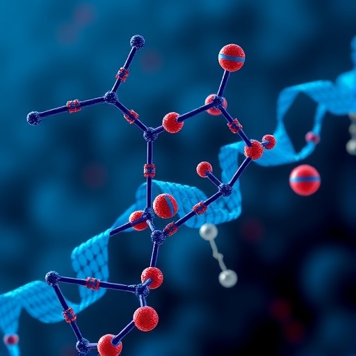
Complex 3D nanoscale architectures based on DNA self-assembly can conduct electricity without resistance and may provide a platform for fabricating quantum computing and sensing devices

Credit: Brookhaven National Laboratory
UPTON, NY–Three-dimensional (3-D) nanostructured materials–those with complex shapes at a size scale of billionths of a meter–that can conduct electricity without resistance could be used in a range of quantum devices. For example, such 3-D superconducting nanostructures could find application in signal amplifiers to enhance the speed and accuracy of quantum computers and ultrasensitive magnetic field sensors for medical imaging and subsurface geology mapping. However, traditional fabrication tools such as lithography have been limited to 1-D and 2-D nanostructures like superconducting wires and thin films.
Now, scientists from the U.S. Department of Energy’s (DOE) Brookhaven National Laboratory, Columbia University, and Bar-Ilan University in Israel have developed a platform for making 3-D superconducting nano-architectures with a prescribed organization. As reported in the Nov. 10 issue of Nature Communications, this platform is based on the self-assembly of DNA into desired 3-D shapes at the nanoscale. In DNA self-assembly, a single long strand of DNA is folded by shorter complementary “staple” strands at specific locations–similar to origami, the Japanese art of paper folding.
“Because of its structural programmability, DNA can provide an assembly platform for building designed nanostructures,” said co-corresponding author Oleg Gang, leader of the Soft and Bio Nanomaterials Group at Brookhaven Lab’s Center for Functional Nanomaterials (CFN) and a professor of chemical engineering and of applied physics and materials science at Columbia Engineering. “However, the fragility of DNA makes it seem unsuitable for functional device fabrication and nanomanufacturing that requires inorganic materials. In this study, we showed how DNA can serve as a scaffold for building 3-D nanoscale architectures that can be fully “converted” into inorganic materials like superconductors.”
To make the scaffold, the Brookhaven and Columbia Engineering scientists first designed octahedral-shaped DNA origami “frames.” Aaron Michelson, Gang’s graduate student, applied a DNA-programmable strategy so that these frames would assemble into desired lattices. Then, he used a chemistry technique to coat the DNA lattices with silicon dioxide (silica), solidifying the originally soft constructions, which required a liquid environment to preserve their structure. The team tailored the fabrication process so the structures were true to their design, as confirmed by imaging at the CFN Electron Microscopy Facility and small-angle x-ray scattering at the Complex Materials Scattering beamline of Brookhaven’s National Synchrotron Light Source II (NSLS-II). These experiments demonstrated that the structural integrity was preserved after they coated the DNA lattices.
“In its original form, DNA is completely unusable for processing with conventional nanotechnology methods,” said Gang. “But once we coat the DNA with silica, we have a mechanically robust 3-D architecture that we can deposit inorganic materials on using these methods. This is analogous to traditional nanomanufacturing, in which valuable materials are deposited onto flat substrates, typically silicon, to add functionality.”
The team shipped the silica-coated DNA lattices from the CFN to Bar-Ilan’s Institute of Superconductivity, which is headed by Yosi Yeshurun. Gang and Yeshurun became acquainted a couple years ago, when Gang delivered a seminar on his DNA assembly research. Yeshurun–who over the past decade has been studying the properties of superconductivity at the nanoscale–thought that Gang’s DNA-based approach could provide a solution to a problem he was trying to solve: How can we fabricate superconducting nanoscale structures in three dimensions?
“Previously, making 3-D nanosuperconductors involved a very elaborate and difficult process using conventional fabrication techniques,” said Yeshurun, co-corresponding author. “Here, we found a relatively simple way using Oleg’s DNA structures.”
At the Institute of Superconductivity, Yeshurun’s graduate student Lior Shani evaporated a low-temperature superconductor (niobium) onto a silicon chip containing a small sample of the lattices. The evaporation rate and silicon substrate temperature had to be carefully controlled so that niobium coated the sample but did not penetrate all the way through. If that happened, a short could occur between the electrodes used for the electronic transport measurements.
“We cut a special channel in the substrate to ensure that the current would only go through the sample itself,” explained Yeshurun.
The measurements revealed a 3-D array of Josephson junctions, or thin nonsuperconducting barriers through which superconducting current tunnels. Arrays of Josephson junctions are key to leveraging quantum phenomena in practical technologies, such as superconducting quantum interference devices for magnetic field sensing. In 3-D, more junctions can be packed into a small volume, increasing device power.
“DNA origami has been producing beautiful and ornate 3-D nanoscale structures for almost 15 years, but DNA itself is not necessarily a useful functional material,” said Evan Runnerstrom, program manager for materials design at the U.S. Army Combat Capabilities Development Command Army Research Laboratory of the U.S. Army Research Office, which funded the work in part. “What Prof. Gang has shown here is that you can leverage DNA origami as a template to create useful 3-D nanostructures of functional materials, like superconducting niobium. This ability to arbitrarily design and fabricate complex 3-D-structured functional materials from the bottom-up will accelerate the Army’s modernization efforts in areas like sensing, optics, and quantum computing.”
“We demonstrated a pathway for how complex DNA organizations can be used to create highly nanostructured 3-D superconducting materials,” said Gang. “This material conversion pathway gives us an ability to make a variety of systems with interesting properties–not only superconductivity but also other electronic, mechanical, optical, and catalytic properties. We can envision it as a “molecular lithography,” where the power of DNA programmability is transferred to 3-D inorganic nanofabrication.”
###
This research was supported by the U.S. Department of Defense, Army Research Office; DOE Office of Science; Israeli Ministry of Science and Technology; and Israel Science Foundation. Both CFN and NSLS-II are DOE Office of Science User Facilities. Some imaging studies were carried out at the Imaging Facility of the City University of New York Advanced Science Research Center.
Brookhaven National Laboratory is supported by the U.S. Department of Energy’s Office of Science. The Office of Science is the single largest supporter of basic research in the physical sciences in the United States and is working to address some of the most pressing challenges of our time. For more information, visit https:/
Follow @BrookhavenLab on Twitter or find us on Facebook.
Columbia Engineering
Columbia Engineering, based in New York City, is one of the top engineering schools in the U.S. and one of the oldest in the nation. Also known as The Fu Foundation School of Engineering and Applied Science, the School expands knowledge and advances technology through the pioneering research of its more than 220 faculty, while educating undergraduate and graduate students in a collaborative environment to become leaders informed by a firm foundation in engineering. The School’s faculty are at the center of the University’s cross-disciplinary research, contributing to the Data Science Institute, Earth Institute, Zuckerman Mind Brain Behavior Institute, Precision Medicine Initiative, and the Columbia Nano Initiative. Guided by its strategic vision, “Columbia Engineering for Humanity,” the School aims to translate ideas into innovations that foster a sustainable, healthy, secure, connected, and creative humanity.
Media Contact
Ariana Manglaviti
[email protected]
Related Journal Article
http://dx.

