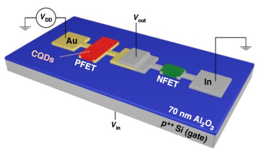
Quantum dot logic circuits provide the long-sought building blocks for innovative devices, including printable electronics, flexible displays, and medical diagnostics

Credit: Los Alamos National Laboratory/University of California, Irvine
LOS ALAMOS, N.M., October 29, 2020 – Researchers at Los Alamos National Laboratory and their collaborators from the University of California, Irvine have created fundamental electronic building blocks out of tiny structures known as quantum dots and used them to assemble functional logic circuits. The innovation promises a cheaper and manufacturing-friendly approach to complex electronic devices that can be fabricated in a chemistry laboratory via simple, solution-based techniques, and offer long-sought components for a host of innovative devices.
“Potential applications of the new approach to electronic devices based on non-toxic quantum dots include printable circuits, flexible displays, lab-on-a-chip diagnostics, wearable devices, medical testing, smart implants, and biometrics,” said Victor Klimov, a physicist specializing in semiconductor nanocrystals at Los Alamos and lead author on a paper announcing the new results in the October 19 issue of Nature Communications.
For decades, microelectronics has relied on extra-high purity silicon processed in a specially created clean-room environment. Recently, silicon-based microelectronics has been challenged by several alternative technologies that allow for fabricating complex electronic circuits outside a clean room, via inexpensive, readily accessible chemical techniques. Colloidal semiconductor nanoparticles made with chemistry methods in much less stringent environments are one such emerging technology. Due to their small size and unique properties directly controlled by quantum mechanics, these particles are dubbed quantum dots.
A colloidal quantum dot consists of a semiconductor core covered with organic molecules. As a result of this hybrid nature, they combine the advantages of well-understood traditional semiconductors with the chemical versatility of molecular systems. These properties are attractive for realizing new types of flexible electronic circuits that could be printed onto virtually any surface including plastic, paper, and even human skin. This capability could benefit numerous areas including consumer electronics, security, digital signage and medical diagnostics.
A key element of electronic circuitry is a transistor that acts as a switch of electrical current activated by applied voltage. Usually transistors come in pairs of n- and p-type devices that control flows of negative and positive electrical charges, respectively. Such pairs of complementary transistors are the cornerstone of the modern CMOS (complementary metal oxide semiconductor) technology, which enables microprocessors, memory chips, image sensors and other electronic devices.
The first quantum dot transistors were demonstrated almost two decades ago. However, integrating complementary n- and p-type devices within the same quantum dot layer remained a long-standing challenge. In addition, most of the efforts in this area have focused on nanocrystals based on lead and cadmium. These elements are highly toxic heavy metals, which greatly limits practical utility of the demonstrated devices.
The team of Los Alamos researchers and their collaborators from the University of California, Irvine have demonstrated that by using copper indium selenide (CuInSe2) quantum dots devoid of heavy metals they were able to address both the problem of toxicity and simultaneously achieve straightforward integration of n- and p-transistors in the same quantum dot layer. As a proof of practical utility of the developed approach, they created functional circuits that performed logical operations.
The innovation that Klimov and colleagues are presenting in their new paper allows them to define p- and n-type transistors by applying two different types of metal contacts (gold and indium, respectively). They completed the devices by depositing a common quantum dot layer on top of the pre-patterned contacts. “This approach permits straightforward integration of an arbitrary number of complementary p- and n-type transistors into the same quantum dot layer prepared as a continuous, un-patterned film via standard spin-coating,” said Klimov.
###
Publication: J. Yun, J. Lim, J. Roh, D. C. J. Neo, M. Law, and V. I. Klimov, Solution-processable integrated CMOS circuits based on colloidal CuInSe2 quantum dots, Nature Communications, DOI: 10.1038/s41467-020-18932-5.
Funding: This work was supported by the Laboratory Directed Research and Development (LDRD) program at Los Alamos National Laboratory under project 20200213DR and the University of California (UC) Office of the President under the UC Laboratory Fees Research Program Collaborative Research and Training Award LFR-17-477148.
About Los Alamos National Laboratory
Los Alamos National Laboratory, a multidisciplinary research institution engaged in strategic science on behalf of national security, is operated by Triad, a public service oriented, national security science organization equally owned by its three founding members: Battelle Memorial Institute (Battelle), the Texas A&M University System (TAMUS), and the Regents of the University of California (UC) for the Department of Energy’s National Nuclear Security Administration.
Los Alamos enhances national security by ensuring the safety and reliability of the U.S. nuclear stockpile, developing technologies to reduce threats from weapons of mass destruction, and solving problems related to energy, environment, infrastructure, health, and global security concerns.
LA-UR-20-28576
Media Contact
James Riordon
[email protected]
Original Source
https:/
Related Journal Article
http://dx.


