Credit: by Chao Qian, Xiao Lin, Xiaobin Lin, Jian Xu, Yang Sun, Erping Li, Baile Zhang, and Hongsheng Chen
Optical logical operations have sparked major interest in the past decades since it can enable many applications, particularly those involving high-throughput and on-the-fly data processing such as secured wireless communication and autonomous driving. However, the reported optical logic gates rely heavily on the precise control of input light/pump light, including the phase, polarization, and amplitude. Due to the complexity and difficulty in these precise controls, the two output states may suffer from an inherent instability and a low contrast ratio of intensity. Moreover, the miniaturization of optical logic gates would become difficult, if the extra bulky apparatus for these controls are considered. As such, it is desirable, albeit challenging, to get rid of these complicated controls and to achieve full logic functionality in a compact photonic system.
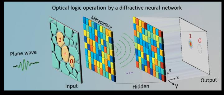
In a new paper published in Light Science & Application, scientists from the Interdisciplinary Center for Quantum Information, Zhejiang University, China, and co-workers introduced a simple yet universal design strategy, namely diffractive neural network, to realize all seven basic optical logic operations in a same compact system, simply using a plane wave as input signal. The diffractive neural network is implemented by a compound Huygens’ metasurface, and it can partially mimic the functionality of artificial neural network. After training, the compound metasurface can directionally scatter or focus the input encoded light into one of the two designated small areas/points, one of which represents logic state ‘1’ and the other stands for ‘0’. As a conceptual demonstration, three basic logic gates, i.e., NOT, OR, and AND, are experimentally verified using a two-layered high-efficiency dielectric metasurface at microwave.
Compared with previous works, this design strategy features two distinct advantages. First, the realization of optical logic operations here gets rid of the complicated and precise control of the features of input light; such a scheme is thus totally different from previous works. Moreover, the design of the input layer is very general and powerful, and it can be flexibly modified into other user-favored and programmable forms. Second, the proposed strategy can enable complete logic functionalities in a single optical network, if the transmittance state of the input layer is simply tunable, e.g., electrically tunable if the optical mask is constructed by a spatial light modulator. Therefore, the revealed universal design strategy has the potential to facilitate a single miniaturized programmable photonic processor for arbitrary logic operations.
The scientists believe that the full-featured optical logical gates make a big step for further miniaturized, high computing density and ultrafast computing element, promised by nanophotonic circuits and meta-structures. Beyond that, the proposed approach will also lead to a broad scope of applications, such as real-time object recognition in surveillance system, and intelligent wave shaping inside biological tissue in microscope imaging.
###
Media Contact
Hongsheng Chen
[email protected]
Related Journal Article
http://dx.


