Scientists explain how perforating flexible electrodes with micrometer-sized holes makes them resistant to bending and folding
Credit: DGIST
The prospect of the widespread commercialization and application of flexible electronics has kept researchers worldwide searching for ingenious ways to enhance their performance and durability. From wearable smart devices to solar cells and health sensors, flexible electronics holds much promise in many engineering fields. Unfortunately, flexible devices are usually as fragile as they look; mechanical deformations, such as bending, can induce the formation and propagation of microscopic cracks that ultimately cause devices to fail.
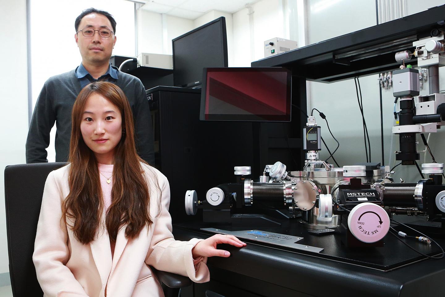
In a recent study, a research team led by Professor Jae Eun Jang from Daegu Gyeongbuk Institute of Science and Technology found a method to greatly improve the durability of thin-film flexible electrodes and transistors, key components in electronics. The method is simple: take your standard flexible conducting film and fill it with micrometer-sized holes in a zigzag pattern.
The researchers actually drew inspiration from civil engineering, as Prof. Jang explains. “We happened to be passing by a construction site, when we saw steel plates with holes, often used in construction. We knew that these steel plates with holes are used to reduce stress. We thought that this method could also be a solution in the micrometer world and, based on this idea, we began conducting experiments.” In the field of mechanics, the word “stress” refers to the forces that the particles of a material exert on each other. External forces increase the stress of a material and can induce the formation of cracks.
In regular thin-film flexible conductors, cracks form in random locations when bent. However, if the flexible conductor bears the array of micrometer-sized holes, the stress distribution of the material changes so that cracks only form at specific points near the edges of the holes and propagate over a short distance. This, as proved through simulations and experiments, allowed their flexible metal electrodes to endure thousands of bending motions. Professor Jang states: “Our devices were able to maintain conductivity up to 300,000 bending cycles, which means that they can be bent over 80 times a day for 10 years.” What’s more, compared with other methods for improving the durability of flexible electronic devices, the proposed approach is inexpensive and easy to adopt using equipment already employed in the display industry.
###
Reference
Authors: Gwang Jun Lee1, Su Jin Heo1, Seungchul Lee1,2, Jae Hoon Yang1, Byoung Ok Jun1, Hyun Sik Kim3 and Jae Eun Jang*1
Title of original paper: Stress Release Effect of Micro-hole Array for Flexible Electrode and Thin Film Transistor
Journal: ACS Applied Materials & Interfaces
DOI: 10.1021/acsami.0c02362
Affiliations: 1Department of Information and Communication Engineering, Daegu Gyeongbuk Institute of Science and Technology (DGIST)
2Samsung Electronics
3Department of Materials Science and Engineering, Hongik University
*Corresponding author’s email: [email protected]
About Daegu Gyeongbuk Institute of Science and Technology (DGIST)
Daegu Gyeongbuk Institute of Science and Technology (DGIST) is a well-known and respected research institute located in Daegu, Republic of Korea. Established in 2004 by the Korean Government, the main aim of DGIST is to promote national science and technology, as well as to boost the local economy.
With a vision of “Changing the world through convergence”, DGIST has undertaken a wide range of research in various fields of science and technology. DGIST has embraced a multidisciplinary approach to research and undertaken intensive studies in some of today’s most vital fields. DGIST also has state-of-the-art-infrastructure to enable cutting-edge research in materials science, robotics, cognitive sciences, and communication engineering.
Website: https:/
About the author
Jae Eun Jang received a Ph.D. degree in Electrical Engineering from the University of Cambridge, U.K. in 2006. After working at Samsung Advanced Institute of Technology, he joined DGIST, Daegu, Korea, as a Professor in Information and Communication Engineering in 2011. Since 2019, he serves as the Associate Vice President for Strategic Planning. He first demonstrated mechanical nanoswitch in 2004, and mechanical DRAM concepts in 2008, using vertically aligned carbon nanotubes. Recently, he was involved in nanodevices for ultra-fast driving, biomimicry concepts, and brain-machine interfaces. He has authored over 200 journal and conference papers and is an inventor of 100 granted patents.
Media Contact
Kwanghoon Choi
[email protected]
Original Source
https:/
Related Journal Article
http://dx.
