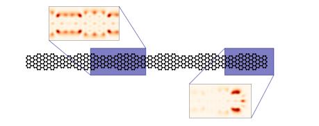
Physicists from Kiel and Copenhagen elucidate the behaviour of electrons in graphene nanoribbons

Credit: Copyright: Jan-Philip Joost, AG Bonitz
New materials are needed to further reduce the size of electronic components and thus make devices such as laptops and smartphones faster and more efficient. Tiny nanostructures of the novel material graphene are promising in this respect. Graphene consists of a single layer of carbon atoms and, among other things, has a very high electrical conductivity. However, the extreme spatial confinement in such nanostructures influences strongly their electronic properties. A team led by Professor Michael Bonitz of the Institute for Theoretical Physics and Astrophysics (ITAP) at Kiel University has now succeeded in simulating the detailed behavior of electrons in these special nanostructures using an elaborate computational model. This knowledge is crucial for the potential use of graphene nanostructures in electronic devices.
Precise simulation of the properties of electrons in nanostructures
Last year, two research teams succeeded independently of each other in fabricating narrow, atomically precise graphene nanoribbons and measuring their electron energies. The width of the nanoribbons varies in a precisely controlled manner. Each section of the nanoribbons has its own energy states with their own electronic structure. “However, the measurement results could not be completely reproduced by previous theoretical models,” says Bonitz, who heads the Chair of Statistical Physics at ITAP. Together with his Ph.D. student Jan-Philip Joost and their Danish colleague Professor Antti-Pekka Jauho from the Technical University of Denmark (DTU), they developed an improved model which led to an excellent agreement with the experiments. The physicists present their theoretical results in the current issue of the renowned journal Nano Letters.
The basis for the new and more precise computer simulations was the assumption that the deviations between the experiment and previous models were caused by the details of the mutual repulsion of the electrons. Although this Coulomb interaction also exists in metals, and indeed was included in earlier simulations in a rough way, the effect is much greater in the small graphene nanoribbons, and requires a detailed analysis. The electrons are expelled from their original energy states and have to ‘search’ for other places, as Bonitz explains: “We were able to prove that correlation effects due to the Coulomb interaction of the electrons have a dramatic influence on the local energy spectrum”.
The shape of nanoribbons determines their electronic properties
How the permissible energy values of the electrons depend on the length, width, and shape of the nanostructures has been clarified by the team by investigating many such nanoribbons. “The energy spectrum also changes when the geometry of the nanoribbons, their width, and shape, is modified,” adds Joost. “For the first time, our new data allow precise predictions to be made as to how the energy spectrum can be controlled by specifically varying the shape of the nanoribbons,” says Jauho from the DTU in Copenhagen. The researchers hope that these predictions will now also be tested experimentally and lead to the development of new nanostructures. Such systems can make important contributions to the further miniaturisation of electronics.
###
Original publication:
Jan-Philip Joost, Antti-Pekka Jauho, Michael Bonitz, Correlated Topological States in Graphene Nanoribbon Heterostructures, Nano Letters, (2019)
DOI:10.1021/acs.nanolett.9b04075, https:/
Photos for download:
https:/
Caption: The graphene nanoribbon (center) consists of a single layer of honeycomb carbon atoms. The ribbon is only a few carbon atoms wide and has different electrical properties depending on its shape and width. The local density of the electrons is increased at the edges, as the dark red areas in the boxes show.
Copyright: Jan-Philip Joost, AG Bonitz
Scientific contact:
Prof. Dr. Michael Bonitz
Institut für Theoretische Physik und Astrophysik
Tel.: +49 431-880-4122
Mail: [email protected]
Web: http://www.
Details, which are only a millionth of a millimetre in size: this is what the priority research area “Kiel Nano, Surface and Interface Science – KiNSIS” at Kiel University has been working on. In the nano-cosmos, different laws prevail than in the macroscopic world – those of quantum physics. Through intensive, interdisciplinary cooperation between physics, chemistry, engineering and life sciences, the priority research area aims to understand the systems in this dimension and to implement the findings in an application-oriented manner. Molecular machines, innovative sensors, bionic materials, quantum computers, advanced therapies and much more could be the result. More information at http://www.
Media Contact
Michael Bonitz
[email protected]
49-431-880-4122
Original Source
http://www.
Related Journal Article
http://dx.


