A new class of sensor interfaces cuts down the design effort from months to hours, reduces circuit complexity by at least 30 times, while being highly robust against wide fluctuations in power harvested from the environment
Credit: National University of Singapore
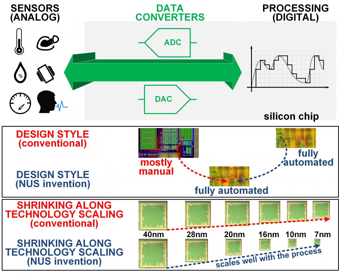
The Green IC research group in the Department of Electrical and Computer Engineering at the National University of Singapore’s (NUS) Faculty of Engineering invented a novel class of Digital-to-Analog (DAC) and Analog-to-Digital Converters (ADC) that can be entirely designed with a fully-automated digital design methodology, thanks to its fully-digital architecture (Fig. 1).
Compared to traditional analog architectures and methodologies, the design turnaround time for these novel sensor interfaces is reduced from months to hours. The drastic reduction in the design effort is highly beneficial in cost-sensitive silicon systems, such as sensors for the Internet of Things (IoT). The novel data converter architecture also has very low complexity, reducing the silicon area and hence the manufacturing cost by at least 30 times, compared to conventional designs.
Such novel data converters also exhibit the unprecedented capability of gracefully degrading the signal fidelity when its supply voltage or clock frequency experience wide fluctuations (Fig. 2). Such fluctuations are common in energy-harvested IoT sensors, being that the power harvested from the surrounding environment (e.g., solar cell) is highly erratic. In turn, this allows uninterrupted sensor signal monitoring even under unfavourable harvested power conditions, and without voltage regulation. Instead, traditional data converters suffer from catastrophic resolution degradation when the supply voltage is below its minimum rated value Vmin (or the frequency exceeds its maximum rated value) as in Fig. 2, hence needing power-hungry circuits for voltage and frequency regulation.
The research was conducted in collaboration with Associate Professor Paolo Crovetti from the Politecnico di Torino in Italy, and is supported by the Singapore Ministry of Education and the EU Commission.
Smaller sensor interfaces, simpler and faster to design
“Our research transforms the traditionally analog and mostly-manual design of data converters into fully-automated digital design, reducing the silicon area by an order of magnitude and the design time by two orders of magnitude, allowing semiconductor companies to be cost-competitive while reaching markets faster,” said the team leader Associate Professor Massimo Alioto, who is from the Department of Electrical and Computer Engineering at the NUS Faculty of Engineering.
He added, “Being digital, our sensor interfaces are effortlessly ported across manufacturing technologies and applications, and can be immersed in digital circuits to avoid the traditional effort required by their integration on the same silicon chip.” (Fig. 1).
The NUS team demonstrated the concept through several silicon chips implementing both DACs and ADCs with extremely low area. As an example, a 12-bit DAC manufactured in 40nm standard CMOS technology has been demonstrated with an area equal to the diameter of a strand of human hair. Its inherent amenability for technology scaling makes it shrink by approximately another 32 times when implemented in the currently finest technology (7 nm).
At the same time, the NUS invention has been shown to enable data converters with high resolutions (up to 16 bits), while achieving design simplicity and compactness.
Team member Dr Orazio Aiello, who is a visiting research fellow at the Department, said, “Our team has introduced a new design paradigm that pushes us closer to the ultimate vision of inexpensive, technology-scalable and ultra-compact IoT devices.”
Unprecedented robustness brings additional benefits at the system level
The NUS innovation further simplifies integrated system design, leveraging the unprecedented ability to withstand very substantial voltage and frequency fluctuations, thus relaxing the accuracy requirements in voltage and frequency generation.
Indeed, conventional data converters operating at a supply voltage below its minimum rated value (or excessive clock frequency) experiences catastrophic failure, and hence fails to perform its intended function (Fig. 2). On the contrary, the innovative data converters invented by the NUS team exhibit graceful degradation of the resolution and signal fidelity when supply voltage or clock frequency exceeds its allowed range. As an example, a DAC designed for 1 V was demonstrated to correctly operate at half this voltage, while degrading its resolution by only 1 bit when the supply voltage is reduced by a substantial 0.3V.
Assoc Prof Alioto said, “The capability of having graceful resolution degradation under voltage and frequency overscaling suppresses the need for complex circuit solutions that accurately regulate the supply voltage and the clock frequency being utilised by data converters. In other words, our data converters are simpler to design, and also simplify the system that they are employed in.”
Next steps
The team is currently working on a novel paradigm that turns traditionally analog and design-intensive silicon sub-systems into digital standard cell-based designs that are supported by fully-automated design flows, pushing the boundary of classical digitally-assisted design. This research study involves several fundamental sub-systems such as amplifiers, oscillators, voltage and current references, and many others.
The research team aims to transform the way integrated systems are designed, enabling ultra-rapid, ultra-compact and technology-portable design of entire systems.
###
Media Contact
Carolyn Fong
[email protected]
65-651-65399
Related Journal Article
http://dx.
