Credit: Brookhaven National Laboratory
New Haven, Conn. – The revolutionary tech discoveries of the next few decades, the ones that will change daily life, may come from new materials so small they make nanomaterials look like lumpy behemoths.
These new materials will be designed and refined at the picometer scale, which is a thousand times smaller than a nanometer and a million times smaller than a micrometer (which itself is smaller than the width of a human hair). In order to do this work, scientists will need training in an array of new equipment that can measure and guide such exquisitely controlled materials. The work involves designing the materials theoretically, fabricating them, and characterizing their properties.
At Yale University, they have a name for it; they call it “picoscience.”
“Researchers at Yale are inventing new materials that are small, fast, and can perform in a multitude of ways, such as mimicking neurons in the brain, computing with magnets, and calculating with quantum mechanics,” said Frederick Walker, a senior research scientist in the lab of Charles Ahn, the John C. Malone Professor of Applied Physics, Mechanical Engineering and Materials Science, and Physics, and chair of the Department of Applied Physics.
Ahn is senior author of a new study that moves picoscience in yet another direction: taking elements from the periodic table and tinkering with them at the subatomic level to tease out new materials.
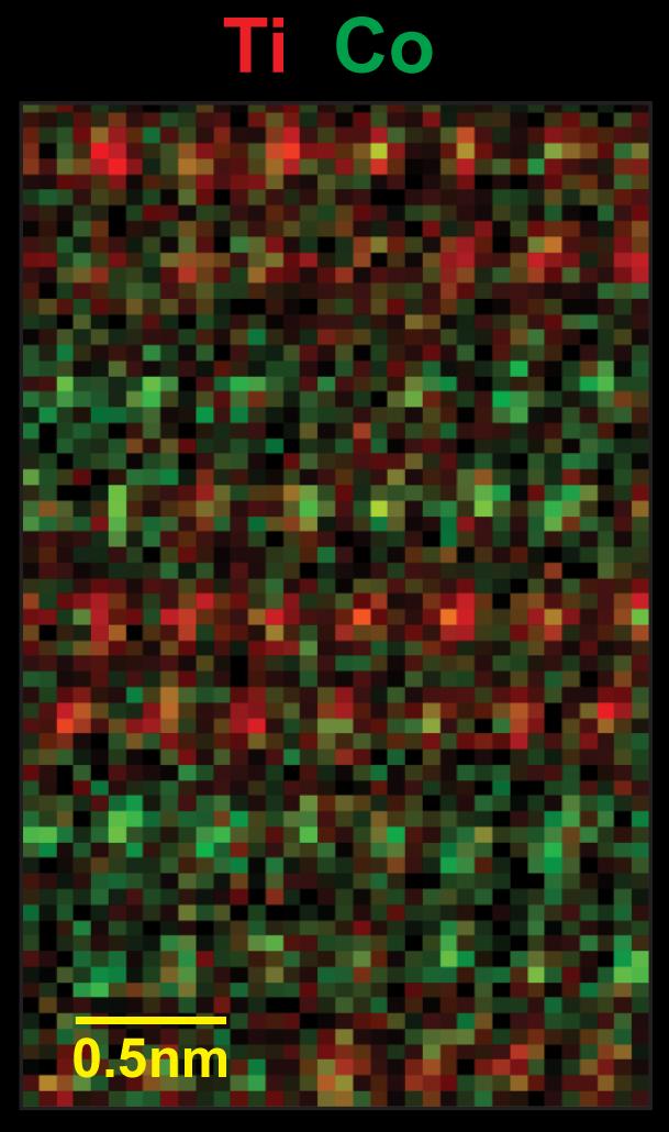
Sangjae Lee, a graduate student in Ahn’s lab and first author of the study, designed and grew the new material, which is an artificial, layered crystal composed of the elements lanthanum, titanium, cobalt, and oxygen.
The researchers layered the elements one atomic plane at a time, so that one-atom-thick sheets of titanium oxide transfer an electron to one-atom-thick-sheets of cobalt oxide. This changed the electronic configuration and magnetic properties of the cobalt oxide sheet.
“We were able to manipulate the constituent atoms with a precision much smaller than the atom itself,” Lee said. “These types of new crystals may form the basis for developing new magnetic materials, where a delicate balance between magnetism and electronic conduction at such small length scales can be manipulated in novel, transistor-like devices that have performance advantages over today’s transistors.”
Lee trained on a number of instruments that are being developed at the National Synchrotron Light Source II at Brookhaven National Laboratory in New York. A synchrotron is a machine roughly the size of a football field that speeds up electrons almost to the speed of light. The electrons generate extremely bright x-ray beams that are used by researchers in experiments.
The new study appears in the journal Physical Review Letters and features co-authors from Yale, Brookhaven, the Flatiron Institute, and Argonne National Laboratory. The Yale co-authors, in addition to Ahn and Lee, are Sohrab Ismail-Beigi, Alex Taekyung Lee, Walker, Ankit Disa, and Yichen Jia.
In addition to designing and growing the new materials, Sangjae Lee characterized them and analyzed the results. From the theoretical side, Yale colleagues Alex Taekyung Lee and Alexandru Georgescu, who is now at the Center for Computational Quantum Physics at the Flatiron Institute, used quantum mechanical computations to compute the structure of the materials and its effect on their electronic configuration. This work enabled the team to describe the magnetic state of the materials.
Yale has identified the development of quantum materials as a priority research area, foreseeing their use in new computational systems that will far outstrip today’s computers. The university also has noted the significance of collaborations with Brookhaven, which has some of the most advanced materials characterization facilities in the United States, including the nation’s newest synchrotron.
“The invention of new materials has been at the heart of technological advances that have transformed our lives,” said co-author Ismail-Beigi, a professor of applied physics at Yale. “New electronic materials have driven the ever-increasing capabilities of cell phones, computers, tablets, smart watches, and medical devices.”
Co-author Walker stressed the importance of communication between experimentalists and theorists in conducting picoscience research: “A synergistic feedback loop between theoretical design and experimental fabrication is crucial to successfully discovering new materials properties,” he said. “This feedback loop has become a signature of the National Science Foundation’s materials discovery program and was originally developed at Yale.”
###
The work was supported by the U.S. Air Force Office of Scientific Research, the National Science Foundation, and the U.S. Department of Energy’s Office of Basic Energy Sciences.
Media Contact
Fred Mamoun
[email protected]
203-436-2643


