Credit: Mark Lopez/Argonne National Laboratory
When exposed to stress and strain, materials can display a wide range of different properties. By using sound waves, scientists have begun to explore fundamental stress behaviors in a crystalline material that could form the basis for quantum information technologies. These technologies involve materials that can encode information in a number of states simultaneously, allowing for more efficient computation.
In a new discovery by researchers at the U.S. Department of Energy’s Argonne National Laboratory and the Pritzker School of Molecular Engineering (PME) at the University of Chicago, scientists used X-rays to observe spatial changes in a silicon carbide crystal when using sound waves to strain buried defects inside it. The work follows on an earlier recent study in which the researchers observed changes in the spin state of the defect’s electrons when the material was similarly strained.
“We’re directly imaging sound’s footprint going through this crystal.” — Argonne materials scientist and Pritzker School of Molecular Engineering staff scientist Joseph Heremans
Because these defects are well isolated within the crystal, they can act as a single molecular state and as carriers of quantum information. When the electrons trapped near the defects change between spin states, they emit energy in the form of photons. Depending on which state the electrons are in, they emit either more or fewer photons in a technique known as spin-dependent readout.
In the experiment, the researchers sought to assess the relationship between the sound energy used to produce the strain on the defects in the crystal lattice and the spin transitions indicated by the emitted photons. While the defects in the crystal naturally fluoresce, the additional strain causes the ground spin of the electron to change state, resulting in a coherent manipulation of the spin state that can be measured optically.
“We wanted to see the coupling between the sound strain and the light response, but to see exactly what the coupling between them is, you need to know both how much strain you’re applying, and how much more optical response you’re getting out,” said Argonne nanoscientist Martin Holt, the lead author of the study.
The electrodes used to generate the sound waves are roughly five microns in width, far larger than the defects themselves, which consist of two missing atoms known as a divacancy complex. The sound wave strains the defects by alternately pushing and pulling on them, causing the electrons to change their spins.
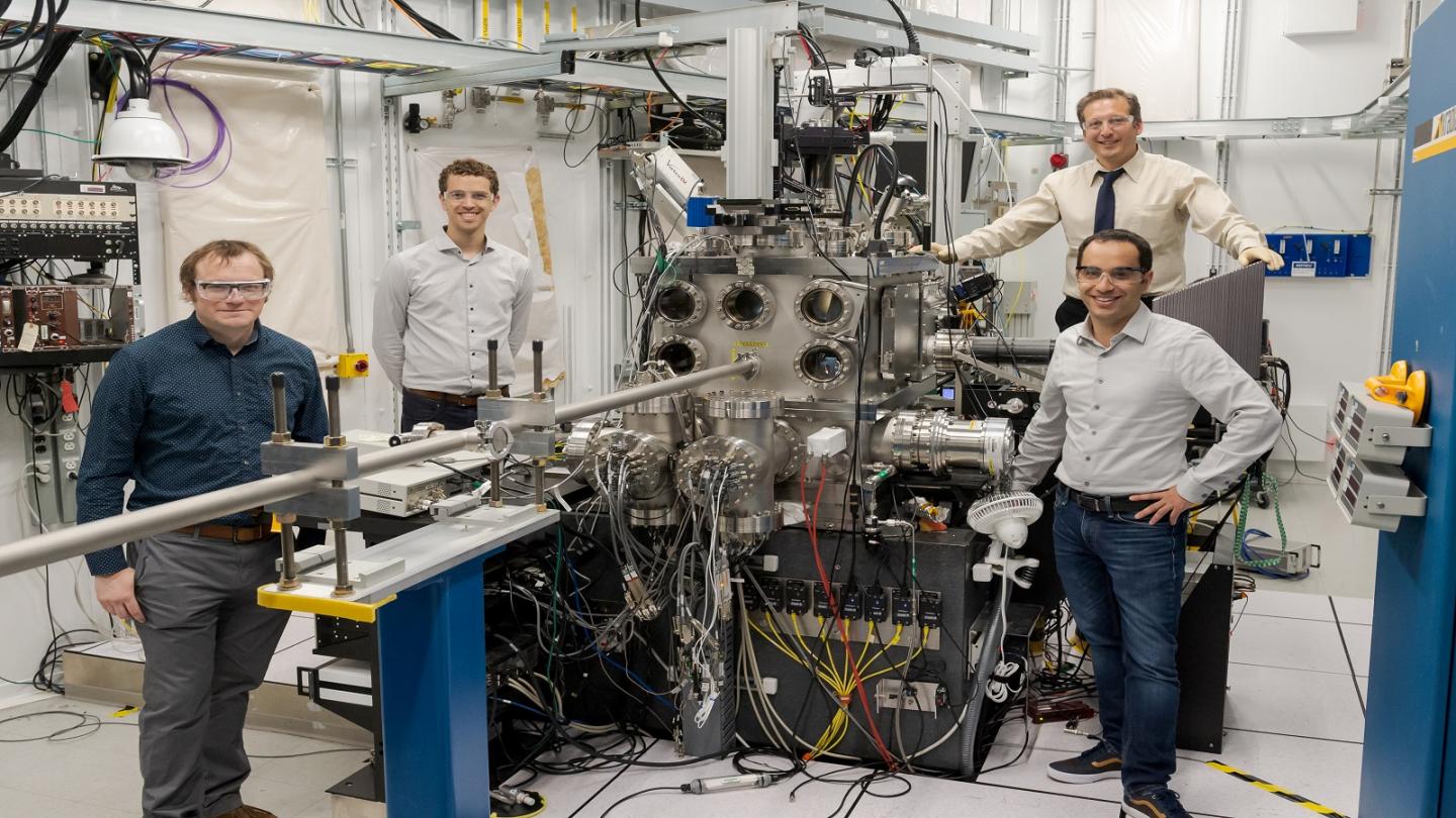
To characterize the lattice and defects, Argonne researchers used the Hard X-ray Nanoprobe beamline operated jointly at the laboratory’s Center for Nanoscale Materials and Advanced Photon Source (APS), both DOE Office of Science User Facilities. Through a newly developed technique called stroboscopic Bragg diffraction microscopy, Holt and his colleagues were able to image the lattice around the defects at many different points throughout the strain cycle.
“We’re interested in how to manipulate the original spin state with acoustic waves, and how you can spatially map out the mechanics of the strain with X-rays,” said Argonne materials scientist and PME staff scientist Joseph Heremans, another author of the study.
“The X-rays measure exactly the lattice distortion,” Holt added.
Stroboscopic Bragg diffraction involves synchronizing the frequency of the acoustic wave to the frequency of the electron pulses in the APS’s storage ring. In this way, the researchers were essentially able to “freeze the wave in time,” according to Holt. This allowed them to create a series of images of the strain experienced by the lattice at each point on the wave.
“It’s like if you had ripples in a pond, and you could shine a light on one spot of the pond,” Holt said. “You’d see a movement of peak to trough, and trough to peak.”
“We’re directly imaging sound’s footprint going through this crystal,” Heremans added. “The sound waves cause the lattice to curve, and we can measure exactly how much the lattice curves by going through a specific point of the lattice at a specific point in time.”
The use of stroboscopic Bragg diffraction allows scientists to determine the direct correlation between the dynamic strain and the quantum behavior of the defect, Holt said. In silicon carbide, this relationship is fairly well understood, but in other materials the technique could reveal surprising relationships between strain and other properties.
“This technique opens a way for us to figure out the behaviors in a lot of systems in which we don’t have a good analytical prediction of what the relationship should be,” Holt said.
“This study combines expertise from a leading academic institution with state-of-the-art instrumentation of a national laboratory to develop a novel technique for probing matter at the atomic scale, revealing the ability of sound waves to control semiconductor quantum technologies,” added Argonne senior scientist and PME Liew Family Professor of Molecular Engineering David Awschalom, a collaborator on the research.
###
A paper based on the study, “Correlating dynamic strain and photoluminescence of solid-state defects with stroboscopic X-ray diffraction microscopy,” appeared in the July 29 online edition of Nature Communications.
Additional collaborators included Samuel Whiteley and Gary Wolfowicz, researchers at both Argonne and the University of Chicago.
The work was funded by the DOE’s Office of Science and the Air Force Office of Scientific Research.
About Argonne’s Center for Nanoscale Materials
The Center for Nanoscale Materials is one of the five DOE Nanoscale Science Research Centers, premier national user facilities for interdisciplinary research at the nanoscale supported by the DOE Office of Science. Together the NSRCs comprise a suite of complementary facilities that provide researchers with state-of-the-art capabilities to fabricate, process, characterize and model nanoscale materials, and constitute the largest infrastructure investment of the National Nanotechnology Initiative. The NSRCs are located at DOE’s Argonne, Brookhaven, Lawrence Berkeley, Oak Ridge, Sandia and Los Alamos National Laboratories. For more information about the DOE NSRCs, please visit https:/
Argonne National Laboratory seeks solutions to pressing national problems in science and technology. The nation’s first national laboratory, Argonne conducts leading-edge basic and applied scientific research in virtually every scientific discipline. Argonne researchers work closely with researchers from hundreds of companies, universities, and federal, state and municipal agencies to help them solve their specific problems, advance America’s scientific leadership and prepare the nation for a better future. With employees from more than 60 nations, Argonne is managed by UChicago Argonne, LLC for the U.S. Department of Energy’s Office of Science.
The U.S. Department of Energy’s Office of Science is the single largest supporter of basic research in the physical sciences in the United States and is working to address some of the most pressing challenges of our time. For more information, visit https:/
Media Contact
Diana Anderson
[email protected]
Original Source
https:/
Related Journal Article
http://dx.


