Two-dimensional semiconductors, heralded as the next generation in semiconductor technology, are characterized by their single atomic layer thickness. Due to their ultra-thin structure, two-dimensional semiconductors exhibit remarkable optical properties and provide flexibility, along with excellent integration capability with other materials, for a wide range of applications. Leveraging these attributes, they are being applied in diverse fields such as advanced flexible devices, nanophotonic devices, and solar cells. A key aspect of the optical characteristics in two-dimensional semiconductors is the presence of excitons, which are electron-hole pairs. Harnessing the generation and recombination of these excitons opens avenues for the development of light-emitting devices and various optical and electronic applications. Another significant optical phenomenon involves the precise control of trions, which are charged excitons. The manipulation of trions offers numerous functionalities for device applications.

Credit: POSTECH
Two-dimensional semiconductors, heralded as the next generation in semiconductor technology, are characterized by their single atomic layer thickness. Due to their ultra-thin structure, two-dimensional semiconductors exhibit remarkable optical properties and provide flexibility, along with excellent integration capability with other materials, for a wide range of applications. Leveraging these attributes, they are being applied in diverse fields such as advanced flexible devices, nanophotonic devices, and solar cells. A key aspect of the optical characteristics in two-dimensional semiconductors is the presence of excitons, which are electron-hole pairs. Harnessing the generation and recombination of these excitons opens avenues for the development of light-emitting devices and various optical and electronic applications. Another significant optical phenomenon involves the precise control of trions, which are charged excitons. The manipulation of trions offers numerous functionalities for device applications.
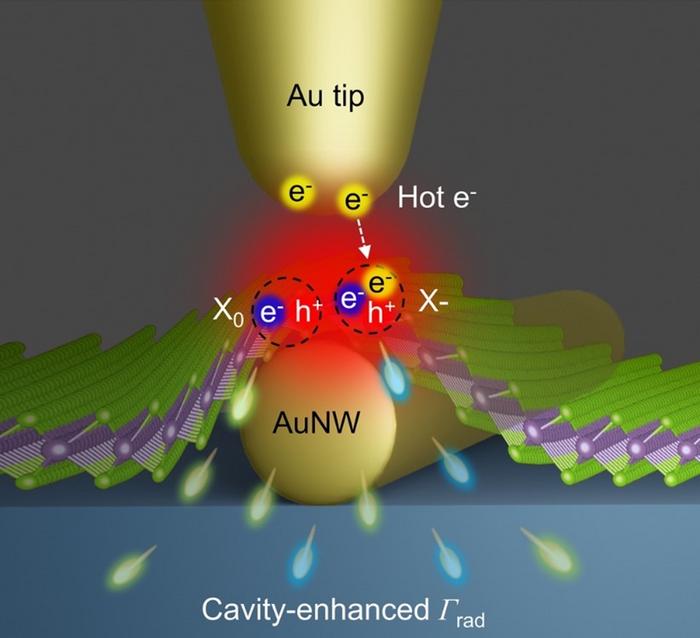
Collaborative research involving Professor Kyoung-Duck Park and Mingu Kang, a PhD candidate, from the Department of Physics at Pohang University of Science and Technology (POSTECH), Professor Yung Doug Suh from the Department of Chemistry at Ulsan National Institute of Science and Technology (UNIST) who is also Deputy Director of the IBS Center for Multidimensional Carbon Materials, and Professor Hyun Seok Lee from the Department of Physics at Chungbuk National University has developed tip-enhanced cavity-spectroscopy system with a gold nanowire structure. This system dynamically manipulates the interconversion of excitons and trions, allowing nanoscale control and investigation of their emission properties. The approach enabled the researchers to successfully discover the mechanism of trion generation.
The integration of metals and semiconductors can lead to the development of multifunctional optoelectronic devices possessing unique optical and electrical properties. The research team fabricated a hybrid structure of gold nanowires with a monolayer of two-dimensional semiconductor, molybdenum diselenide (MoSe2). They also built a tip-enhanced cavity-spectroscopy system, by integrating the hybrid structure with tip-enhanced nano-spectroscopy.
Illumination of laser to the well-designed gold nanowire structure induces the formation of standing waves of plasmons at the surface. Initially, it was intended to induce conversion of excitons to trions in the two-dimensional semiconductor, but the multipole mode was found to contribute to the conversion process. The tip-enhanced cavity-spectroscopy system facilitates the investigation of optical properties of excitons and trions at the nanoscale by achieving a spatial resolution of approximately 10 nm, which is surpassing optical diffraction limits. This system can reveal the underlying principles of trion generation and enable the dynamic manipulation of exciton-trion interconversion in a reversible manner.
Moreover, the dynamically controlled gold tip, which concentrates light within a nanoscale region, generates high-energy hot electrons. These electrons can be injected into the two-dimensional semiconductor, affecting the generation of trions. This approach not only led to the development of high-precision measurement tools that enable the manipulation of materials with ultra-high resolution, but also prompted the researchers to propose a novel platform for the control of excitons and trions in semiconductors at the nanoscale.
Mingu Kang, the lead author of the research, remarked, “We successfully demonstrate the nanoscale manipulation of excitons and trions, and reveal the principles governing the interaction between excitonic quasiparticles, plasmons, and hot electrons.” He added, “This breakthrough could open new avenues for optoelectronic device applications using excitons and trions such as solar cells and photoelectric integrated circuits.”
Su Jin Kim from the Department of Physics at Chungbuk National University, and Huitae Joo, Yeonjeong Koo, and Hyeongwoo Lee, integrated PhD students at the POSTECH, were contributors to the research. The research, recently published in the international journal Nano Letters, was sponsored by the National Research Foundation of Korea, the Ministry of Science and ICT, the Electronics and Telecommunications Research Institute, the Samsung Future Technology Incubation Program, the Commercializations Promotion Agency for R&D Outcomes, the Korea Research Institute of Chemical Technology, the UNIST, and the Institute for Basic Science (IBS).
Journal
Nano Letters
DOI
10.1021/acs.nanolett.3c03920
Article Title
Nanoscale Manipulation of Exciton–Trion Interconversion in a MoSe2 Monolayer via Tip-Enhanced Cavity-Spectroscopy
Article Publication Date
10-Jan-2024


