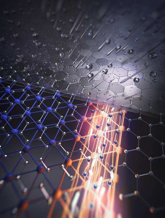
The race to create increasingly faster and more powerful computer chips continues as transistors, their fundamental components, shrink to ever smaller and more compact sizes. In a few years, these transistors will measure just a few atoms across – by which point, the miniaturization of the silicon technology currently used will have reached its physical limits. Consequently, the quest for alternative materials with entirely new properties is crucial for future technological advancements.
Credit: Jörg Bandmann, pixelwg
The race to create increasingly faster and more powerful computer chips continues as transistors, their fundamental components, shrink to ever smaller and more compact sizes. In a few years, these transistors will measure just a few atoms across – by which point, the miniaturization of the silicon technology currently used will have reached its physical limits. Consequently, the quest for alternative materials with entirely new properties is crucial for future technological advancements.
Back in 2021, scientists from the Cluster of Excellence ct.qmat – Complexity and Topology in Quantum Matter at the universities JMU Würzburg and TU Dresden made a significant discovery: topological quantum materials such as indenene, which hold great promise for ultrafast, energy-efficient electronics. The resulting, extremely thin quantum semiconductors are composed of a single atom layer – in indenene’s case, indium atoms – and act as topological insulators, conducting electricity virtually without resistance along their edges.
“Producing such a single atomic layer requires sophisticated vacuum equipment and a specific substrate material. To utilize this two-dimensional material in electronic components, it would need to be removed from the vacuum environment. However, exposure to air, even briefly, leads to oxidation, destroying its revolutionary properties and rendering it useless,” explains experimental physicist Professor Ralph Claessen, ct.qmat’s Würzburg spokesperson.
The ct.qmat Würzburg team has now managed to solve this problem. Their results have been published in the journal Nature Communications.
In Search of a Protective Coating
“We dedicated two years to finding a method to protect the sensitive indenene layer from environmental elements using a protective coating. The challenge was ensuring that this coating did not interact with the indenene layer,” explains Cedric Schmitt, one of Claessen’s doctoral students involved in the project. This interaction is problematic because when different types of atoms – from the protective layer and the semiconductor, for instance – meet, they react chemically at the atomic level, changing the material. This isn’t a problem with conventional silicon chips, which comprise multiple atomic layers, leaving sufficient layers unaffected and hence still functional.
“A semiconductor material consisting of a single atomic layer such as indenene would normally be compromised by a protective film. This posed a seemingly insurmountable challenge that piqued our research curiosity,” says Claessen. The search for a viable protective layer led them to explore van der Waals materials, named after the Dutch physicist Johannes Diderik van der Waals (1837–1923). Claessen explains: “These two-dimensional van der Waals atomic layers are characterized by strong internal bonds between their atoms, while only weakly bonding to the substrate. This concept is akin to how pencil lead made of graphite – a form of carbon with atoms arranged in honeycomb layers – writes on paper. The layers of graphene can be easily separated. We aimed to replicate this characteristic.”
Success!
Using sophisticated ultrahigh vacuum equipment, the Würzburg team experimented with heating silicon carbide (SiC) as a substrate for indenene, exploring the conditions needed to form graphene from it. “Silicon carbide consists of silicon and carbon atoms. Heating it causes the carbon atoms to detach from the surface and form graphene,” says Schmitt, elucidating the laboratory process. “We then vapor-deposited indium atoms, which are immersed between the protective graphene layer and the silicon carbide substrate. This is how the protective layer for our two-dimensional quantum material indenene was formed.”
Umbrella Unfurled
For the first time globally, Claessen and his team at ct.qmat’s Würzburg branch successfully crafted a functional protective layer for a two-dimensional quantum semiconductor material without compromising its extraordinary quantum properties. After analyzing the fabrication process, they thoroughly tested the layer’s protective capabilities against oxidation and corrosion. “It works! The sample can even be exposed to water without being affected in any way,” says Claessen with delight. “The graphene layer acts like an umbrella for our indenene.”
Toward Atomic Layer Electronics
This breakthrough paves the way for applications involving highly sensitive semiconductor atomic layers. The manufacture of ultrathin electronic components requires them to be processed in air or other chemical environments. This has been made possible thanks to the discovery of this protective mechanism. The team in Würzburg is now focused on identifying more van der Waals materials that can serve as protective layers – and they already have a few prospects in mind. The snag is that despite graphene’s effective protection of atomic monolayers against environmental factors, its electrical conductivity poses a risk of short circuits. The Würzburg scientists are working on overcoming these challenges and creating the conditions for tomorrow’s atomic layer electronics.
Cluster of Excellence ct.qmat
The Cluster of Excellence ct.qmat – Complexity and Topology in Quantum Matter has been jointly run by Julius-Maximilians-Universität (JMU) Würzburg and Technische Universität (TU) Dresden since 2019. Over 300 scientists from more than thirty countries and four continents study topological quantum materials that reveal surprising phenomena under extreme conditions such as ultra-low temperatures, high pressure, or strong magnetic fields. ct.qmat is funded through the German Excellence Strategy of the Federal and State Governments and is the only Cluster of Excellence in Germany to be based in two different federal states.
Journal
Nature Communications
DOI
10.1038/s41467-024-45816-9
Article Title
Achieving environmental stability in an atomically thin quantum spin Hall insulator via graphene intercalation device
Article Publication Date
19-Feb-2024
COI Statement
No Conflict of Interest


