

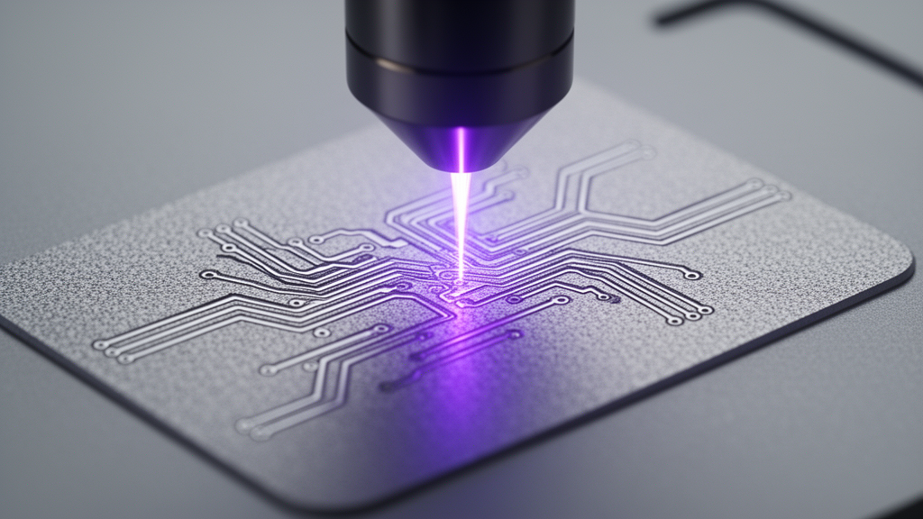
Ultraviolet nanosecond laser processing operating at a wavelength of 355 nanometers provides a practical, maskless platform for printed circuit board prototyping, direct copper ablation, polymer surface conditioning, and selective surface activation before metallization, according to an integrative narrative synthesis published in Discover Electronics by researcher Richard Berenyi. The comprehensive review evaluates finite element modelling of copper ablation, direct micro-structuring of standard glass-fibre-reinforced epoxy laminate boards known as FR4, and the interaction of ultraviolet beams with polylactic acid composites. By examining the fundamental light-matter interactions and process limits across four anchor studies and broader supplementary literature, the synthesis establishes how localized, programmable energy delivery can address emerging manufacturing needs while navigating the demanding thermal and chemical constraints of both legacy and green electronic substrates.
Advanced electronics manufacturing currently faces conflicting demands, driven simultaneously by device miniaturization, accelerated product development cycles, and the urgent requirement to curb environmental degradation. Miniaturization requires digital tool paths, tight feature definitions, and reduced tooling overhead directly from computer-aided design files, while circular economy mandates demand substrates that generate less waste and facilitate straightforward material recovery at end of life. Data cited from the Global E-waste Monitor indicates that worldwide electronic waste generation expanded from approximately 34 million metric tonnes in 2010 to 62 million metric tonnes in 2022, with forecasts projecting a rise to 82 million metric tonnes by 2030. Although printed circuit boards constitute only a fraction of this global mass, they present formidable recycling challenges because metals, structural glass fibres, thermoset resins, brominated flame retardants, and mounted electronic components are densely integrated into an unyielding composite architecture.
To establish how laser tooling interacts across these heterogeneous materials, the author synthesizes transient heat-conduction physics as a primary first-order analytical framework. In this formulation, absorbed pulse energy heats the localized target volume, inducing material modification or removal once specific thermal thresholds for melting, vaporization, decomposition, or chemical activation are crossed. The governing differential equation balances material density, specific heat capacity, and thermal conductivity against volumetric or boundary heat flux sources. For high-conductivity metals such as copper, heat redistributes rapidly into adjacent regions, rendering absorbed energy fractions, inter-pulse cooling intervals, and phase-change thermodynamics critical to feature formation. Conversely, for polymer matrices and biocomposites, optical absorption coefficients at 355 nanometers, organic bond structures, filler additives, and material porosity dominate the interaction, demanding careful co-optimization of pulse energy, repetition rate, and galvanometer scan velocity to prevent unwanted charring or substrate swelling.
Despite the utility of conduction equations, the review emphasizes that treating ultraviolet nanosecond laser interactions as purely thermal processes introduces severe physical limitations. Investigations into polyimide reveal sharply bounded ablation thresholds alongside thermal deformation at elevated fluences, confirming that the absence of visible melt fringes alone does not prove a purely photochemical mechanism. When processing copper, dynamic changes in surface reflectivity, plume shielding, and hydrodynamic melt redistribution cause substantial departures from basic conduction predictions. Consequently, finite element modelling captures the general monotonic rise in ablation depth under successive laser pulses but consistently overestimates copper removal at elevated pulse counts. The synthesis clarifies that these discrepancies stem from idealized model assumptions, including oversimplified energy absorption profiles, threshold removal criteria, neglected recoil pressures, and unmodelled debris accumulation, all of which require experimental validation rather than assumptions based solely on laser wavelength.
The review systematically distinguishes between competing circuit manufacturing workflows, demonstrating that laser processing is not a single interchangeable step but a flexible platform that alters downstream constraints. In conventional FR4 processing, subtractive isolation removes unwanted copper directly from a pre-existing metallic cladding without hazardous wet-etching baths, though it remains prone to debris deposition, localized heat-affected zones, and serial writing throughput limits. Alternatively, hybrid routes utilize laser beams merely to pattern photoresist prior to chemical etching. In additive and sustainable manufacturing, laser direct structuring and selective activation treat polymer surfaces to deposit catalytic seeds that undergo subsequent electroless plating or ink printing. These process routes require entirely different analytical controls: while direct copper isolation demands strict verification of electrical insulation and dielectric undercutting, selective polymer activation requires quantifying chemical functionalization, micro-roughness, catalyst uptake, and interface adhesion.
Evaluating laser source architectures, the synthesis compares 355-nanometer nanosecond sources against competing industrial lasers, concluding that equipment selection represents an application-dependent compromise rather than an absolute hierarchy of cost or wavelength. Ultrashort-pulse systems operating in the green picosecond and femtosecond regimes provide exceptional edge definition and debris-free microvias in multilayer boards, but they carry distinct optical complexity and operational parameters. Near-infrared continuous or pulsed fibre systems have demonstrated circuit prototyping capabilities on polyimide laminates, whereas carbon dioxide lasers have been employed to produce laser-induced graphene on polyimide sheets that are subsequently transferred onto polylactic acid backings via hot compression. The review explicitly cautions that graphene transfer must not be conflated with the direct synthesis of graphene from neat polylactic acid, underscoring that each laser tool must be evaluated across matched metrics of throughput, capital cost, cleaning complexity, and mechanical damage.
When assessing green substrate development, the review positions polylactic acid biopolymers as promising materials for specific low-temperature, short-lifetime applications, but confirms they cannot yet serve as universal replacements for standard FR4 laminates. Polylactic acid offers renewable bio-based origins, lower bulk density, and straightforward processing via additive manufacturing methods such as fused deposition modelling and digital light processing. Nevertheless, its commercial deployment in structural circuit boards is severely constrained by an inherently low glass transition temperature, narrow assembly temperature margins, moisture uptake, low flame retardancy, and poor conductor-matrix interfacial bonding. The synthesis notes that while recyclability has been confirmed for sisal-reinforced biocomposites, hydrothermal ageing tests reveal that environmental moisture penetration significantly degrades natural-fibre composites, restricting immediate commercial deployment to disposable diagnostic sensors, educational demonstrator boards, and low-power wearable devices.
Quantitative sustainability claims within the literature are subjected to rigorous contextual scrutiny to prevent overgeneralized environmental claims. The review highlights recent breakthroughs in recyclable vitrimer circuit boards that achieve recovery rates of 98 percent of resin polymers, 100 percent of reinforcing fibres, and 91 percent of process solvents, stressing that these values represent separate constituent streams that cannot be aggregated into a single figure. Furthermore, additively manufactured boards featuring zinc conductive traces report five-micrometre track resolutions, sheet resistances of three milliohms per square, stable shelf lives exceeding one year, and a 79 percent lower global warming potential relative to standard fiberglass-copper boards. However, the author stresses that this 79 percent reduction is specific to the examined additive zinc growth-and-transfer system and cannot be claimed as an inherent attribute of all ultraviolet-patterned polylactic acid hardware without complete, matched life-cycle assessments.
Reliability engineering and interfacial integrity represent the most decisive technical barriers confronting sustainable laser-processed circuit boards. An isolated trace that exhibits crisp geometric fidelity under optical microscopy may fail catastrophic electrical testing if coefficient-of-thermal-expansion mismatches induce interfacial fatigue cracks or if ambient humidity causes delamination between copper and the bio-based core. Furthermore, introducing flame-retardant additives to achieve regulatory fire resistance frequently compromises matrix crystallization, mechanical resilience, and laser optical absorption. Component assembly introduces additional thermal stress, as standard industrial reflow soldering temperatures exceed the degradation thresholds of untreated polylactic acid. Consequently, practical implementations must employ low-melting-point solder alloys or conductive polymer adhesives, treating component attachment not as a detached downstream task but as a coupled variable within the substrate design window.
The review concludes by proposing an evidence-backed roadmap and prioritized research agenda, emphasizing that future development must advance from isolated proof-of-concept demonstrations to integrated, experimentally verified manufacturing guidelines. Top research priorities identified by the author include establishing standardized reliability testing protocols spanning thermal cycling, mechanical flexing, and humidity-induced impedance drift, followed by rigorous head-to-head comparisons of printing, plating, and subtractive copper isolation on identical substrate formulations. Finite element models must incorporate empirical dynamic absorption, vapor plume shielding, and melt kinetics to achieve true predictive capability, while multivariable statistical designs of experiments should optimize interacting laser parameters. Ultimately, realizing commercially viable, sustainable electronics manufacturing depends on harmonizing laser energy coupling, polymer formulation, metallization chemistry, and full life-cycle economics across clear application-specific operating envelopes.
Subject of Research: Ultraviolet nanosecond laser processing and manufacturing frameworks for conventional and sustainable printed circuit boards
Article Title: UV nanosecond laser processing of conventional and sustainable printed circuit boards
Article References: Berenyi, R. (2026). UV nanosecond laser processing of conventional and sustainable printed circuit boards. Discover Electronics, 3(1), Article 164. https://doi.org/10.1007/s44291-026-00313-9
Image Credits: AI Generated
DOI: 10.1007/s44291-026-00313-9
Keywords: UV nanosecond laser, printed circuit boards, laser ablation, copper structuring, polylactic acid, sustainable electronics, FR4 laminate, finite element modelling, laser direct structuring, surface activation, electronic waste, electroless plating, thermal transport, green substrates, additive manufacturing, circuit reliability
News Source: Denise Maddox. (November 15, 2026). Ultraviolet Nanosecond Lasers Enable Precision Circuit Prototyping on Recyclable Electronics Substrates. Scienmag.