Researchers associated with the University of Electro-Communications and Tohoku University have unveiled groundbreaking results concerning local dipole moments at semiconductor surfaces, particularly focusing on the Si(111) surface. This collaborative effort, spearheaded by Akira Sumiyoshi and Jun Nakamura from the University of Electro-Communications, alongside Kohei Yamasue and Yasuo Cho from Tohoku University, bridges a significant gap in understanding atomic-scale charge distributions. The essence of their findings is rooted in the interplay of experimental techniques and sophisticated modeling, utilizing the scanning nonlinear dielectric microscope (SNDM) effectively combined with rigorous density functional theory (DFT) calculations.
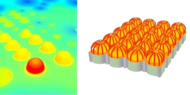
The SNDM technique enables researchers to visualize the intricate landscapes of charge distributions, offering insights that were previously obscured. By rendering the local dipole moments visible, the SNDM provides a unique interface with experimental data that pioneers new pathways for semiconductor analysis. The research specifically observes that the adatom sites on Si(111) surfaces exhibit a distinct upward dipole moment. These observations hold substantial relevance to both the fundamental understanding of semiconductor physics and practical applications.
One of the study’s remarkable aspects is the measurement of how varying local atomic arrangements can significantly alter charge transfer mechanisms. The variances in these structures contribute to the overall dipole moments, which may influence semiconductor behaviors in practical devices. This knowledge is pivotal for scientists and engineers, as an improved comprehension of how atomic arrangements and dipole moments interact can refine device engineering processes, leading to next-generation materials and technologies.
The interplay between theory and experiment in this research serves as a paradigm for future studies in semiconductor science. The empirical data obtained from SNDM correlates almost seamlessly with the theoretical calculations derived from DFT, thereby enhancing the credibility of the simulation methods employed. The researchers emphasized how each aspect of experimentation complements fundamental theoretical insights, thereby providing a well-rounded approach to uncovering the complexities of semiconductor surfaces.
Among the various implications of this study, there lies the potential for advancing semiconductor device fabrication techniques. A deeper understanding of local charge distributions allows for more precise modifications of semiconductor materials, which is essential in an era increasingly dominated by technology. With companies and research institutions racing toward the development of faster and more efficient electronic components, these findings could play a crucial role in cutting-edge semiconductor device engineering.
Furthermore, the implications extend beyond just semiconductor devices. As researchers delve deeper into the realm of material science, insights gleaned from this study might influence other fields such as photovoltaic technology, nanotechnology, and basic materials research. Understanding the coulombic interactions and charge distributions on surfaces opens avenues for innovating and improving current materials used across various industries.
As published in the open-access journal “Scientific Reports,” the study not only democratizes access to groundbreaking research but also invites wider discussions within the scientific community and industry stakeholders. With the publication date set on March 3rd, 2025, this study sets a significant milestone for open scientific dialogue concerning semiconductor research. The authors, with no competing interests, demonstrate a dedication to enhancing knowledge within this vital area of science.
Their use of DFT calculations and advanced modeling techniques illustrates a growing trend in the research community toward integrating computational frameworks with experimental techniques. This dual approach offers robust platforms for hypothesis testing, enabling researchers to predict behaviors and outcomes before empirical validation. Such methodologies are becoming indispensable in the fast-paced world of research, where experimental verification is often costly and time-consuming.
The need for such advanced techniques has never been more apparent as the demand for improved electronic components grows alongside technological advancements. As researchers and developers strive towards creating more efficient, microscopic devices, insights like those from this study will undoubtedly influence the trajectory of electronic device innovation.
The collaboration between different universities not only enriches the research landscape but also paves the way for interdisciplinary studies that could yield even more startling discoveries. The findings presented suggest that further exploration of semiconductor surfaces could lead to groundbreaking shifts in our understanding of electronic materials and their applications.
Overall, the local dipole moment visualization at semiconductor surfaces marks a significant step in semiconductor technology. As researchers continue to dissect and analyze the atomic structures contributing to electronic properties, one can only speculate the myriad of applications such insights might have on future technology innovations. This synergy between experimentation and theory underscores a transformative approach to materials research, placing the scientific community on the brink of discovering new potential in semiconductor physics.
In an age rooted in technology, studies such as these remind us of the inherent complexities in seemingly simple surfaces and the extensive implications they hold for the future. The advancements in understanding local dipole moments and their impacts at the atomic scale are set to revolutionize not only semiconductor technology but also a multitude of applications across various scientific domains.
Subject of Research: Local dipole moments at semiconductor surfaces
Article Title: Visualization of the local dipole moment at the Si(111) surface using DFT calculations
News Publication Date: March 3rd, 2025
Web References: http://dx.doi.org/10.1038/s41598-025-91645-1
References: N/A
Image Credits: N/A
Keywords
Dipole moments, Semiconductor surfaces, Scanning nonlinear dielectric microscope, Density functional theory, Charge distribution, Material science, Electronic devices, SNDM, Atomic arrangements, Semiconductor technology, Research collaboration, Electron microscopy.
Tags: adatom sites dipole momentsadvanced visualization techniques in surface scienceatomic-scale charge distributionscharge transfer mechanisms in semiconductorscollaborative research in semiconductor physicsdensity functional theory calculationsexperimental techniques in material sciencelocal dielectric propertieslocal dipole moments visualizationscanning nonlinear dielectric microscopesemiconductor surface analysisSi(111) surface research


