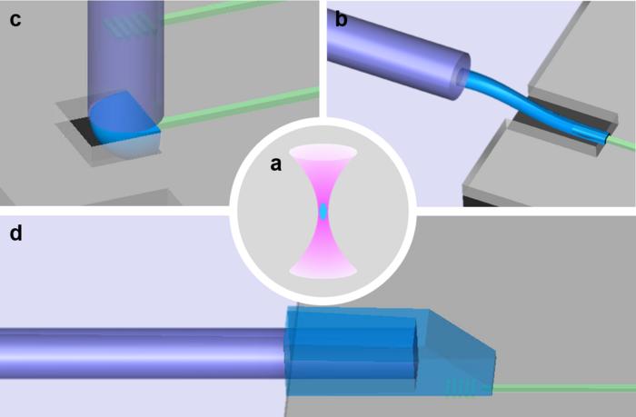
Photonic integrated circuits (PICs) are compact devices that combine multiple optical components on a single chip. They have a wide range of applications in communications, ranging, sensing, computing, spectroscopy, and quantum technology. PICs are now manufactured using mature semiconductor fabrication technologies. It has reduced costs and improved performance. This makes PICs a promising technology for a variety of applications.

Credit: by Shaoliang Yu, Qingyang Du, Cleber Renato Mendonca, Luigi Ranno, Tian Gu and Juejun Hu
Photonic integrated circuits (PICs) are compact devices that combine multiple optical components on a single chip. They have a wide range of applications in communications, ranging, sensing, computing, spectroscopy, and quantum technology. PICs are now manufactured using mature semiconductor fabrication technologies. It has reduced costs and improved performance. This makes PICs a promising technology for a variety of applications.
Photonic packaging is much more challenging than electronic packaging. PICs require much higher alignment accuracy, typically at the micron or even submicron level. This is because the optical modes of PICs need to be precisely matched.
The tight alignment tolerance of PICs makes them incompatible with mainstream electronic packaging techniques and infrastructure. Additionally, the increasing demand for heterogeneous or hybrid integration of multiple material platforms (such as silicon III-V and lithium niobite) is another challenge for photonic packaging. New packaging technologies and device architectures are needed to address these challenges.
In a new paper published in Light Advanced Manufacturing, a team of scientists led by Dr. Shaoliang Yu and Qingyang Du have developed new packaging technologies.
Two-photon lithography (TPL) is a laser-based technology that can be used to create 3D structures with very high resolution. It has recently emerged as a promising approach for photonic packaging, which is the process of assembling and connecting photonic components into a single system.
TPL offers several unique advantages for photonic packaging. TPL can be used to create various 3D photonic structures, such as beam shapers and mode transformers. This is important for achieving high coupling efficiency and wide bandwidths when connecting different optical components in a system.
It can also form optical connections between photonic components after assembly. This is because the shape of the connections can be customized according to the relative displacement between the components. This relaxes the alignment tolerance during PIC assembly and enables the use of standard electronic assembly techniques.
TPL can create high-channel-density, low-loss 2.5-D or 3-D links to accommodate the height differences between the optical ports inside a package. This is particularly important for hybrid integration, in which modules are patterned on different substrates with varying thicknesses.
TPL can be used to form micro- and nano-mechanical structures to guide precise component placement in a passive alignment process or pluggable optical connectors.
In addition to these advantages, TPL resins are typically broadband and low in optical attenuation, making them suitable for building low-loss optical links between dissimilar material platforms.
Overall, TPL is a versatile and powerful technology for photonic packaging. It offers several unique advantages that can help to address the challenges of packaging PICs, such as the tight alignment tolerance and the need for heterogeneous or hybrid integration. As the photonics industry increasingly adopts TPL, further research and development efforts are underway to boost TPL fabrication throughput, expand the material repertoire, and develop new design and characterization tools.
Journal
Light: Advanced Manufacturing
DOI
10.37188/lam.2023.032


