Credit: Penn State College of Engineering
New possibilities for future developments in electronic and optical devices have been unlocked by recent advancements in two-dimensional (2D) materials, according to Penn State researchers.
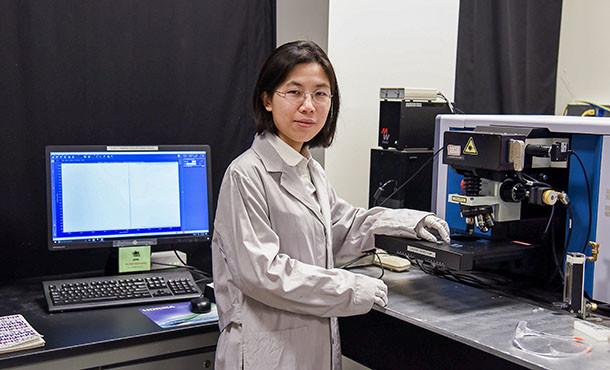
The researchers, led by Shengxi Huang, assistant professor of electrical engineering and biomedical engineering at Penn State, recently published the results of two separate but related discoveries regarding their success with altering the thin 2D materials for applications in many optical and electronic devices. By altering the material in two different ways — atomically and physically — the researchers were able to enhance light emission and increase signal strength, expanding the bounds of what is possible with devices that rely on these materials.
In the first method, the researchers modified the atomic makeup of the materials. In commonly used 2D materials, researchers rely on the interaction between the thin layers, known as van der Waals interlayer coupling, to create charge transfer that is then used in devices. However, this interlayer coupling is limited because the charges are traditionally distributed evenly on the two sides of each layer.
In order to strengthen the coupling, the researchers created a new type of 2D material known as Janus transition metal dichalcogenides by replacing atoms on one side of the layer with a different type of atoms, creating uneven distribution of the charge.
“This [atomic change] means the charge can be distributed unevenly,” Huang said. “That creates an electric field within the plane, and can attract different molecules because of that, which can enhance light emission.”
Also, if van der Waals interlayer coupling can be tuned to the right level by twisting layers with a certain angle, it can induce superconductivity, carrying implications for advancements in electronic and optical devices.
In the second method of altering 2D materials to improve their capabilities, the researchers strengthened the signal that resulted from an energy up-conversion process by taking a layer of MoS2, a common 2D material that is usually flat and thin, and rolling it into a roughly cylindrical shape.
The energy conversion process that takes place with the MoS2 material is part of a nonlinear optical effect where, if a light is shined into an object, the frequency is doubled, which is where the energy conversion comes in.
“We always want to double the frequency in this process,” Huang said. “But the signal is usually very weak, so enhancing the signal is very important.”
By rolling the material, the researchers achieved a more than 95 times signal improvement.
Now, Huang plans to put these two advances together.
“The next step for our research is answering how we can combine atomic engineering and shape engineering to create better optical devices,” she said.
###
A paper on the research of the atomic structure, “Enhancement of van der Waals Interlayer Coupling through Polar Janus MoSSe,” was recently published in the Journal of the American Chemical Society (ACS). The paper on the research of rolling the materials, “Chirality-Dependent Second Harmonic Generation of MoS2-Nanoscroll with Enhanced Efficiency,” was published recently in ACS Nano.
Media Contact
A’ndrea Elyse Messer
[email protected]
Related Journal Article
http://dx.


