Credit: Tokyo Tech
Metal halide perovskites have recently emerged as an exceptionally promising alternative material for next generation optoelectronic applications. Especially, nanoscale-size perovskite structures posse remarkable photophysical properties, such as direct bandgap, color tunability, large absorption cross-section, and narrow photoluminescence linewidth. Together with their low cost, feasibility for scale-up synthesis, solution processability and compatibility with existing optoelectronic device components, these properties make metal halide perovskite nanocrystals a feasible alternative to other semiconducting materials for a range of light-emitting applications including displays, lighting, lasers, as well as memory devices.
However, while perovskite nanocrystals show very high photoluminescence yield, electroluminescence devices prepared from such nanocrystals have long suffered from low efficiency. Recent efforts have concentrated on device engineering to overcome this problem, but there has been so far no systematic study on the nanoscale physical origin of the poor efficiencies. Here, the team of prof. Martin Vacha from Tokyo Tech used single-particle microscopic detection and spectroscopy to study the electroluminescence process on the level of individual nanocrystals.
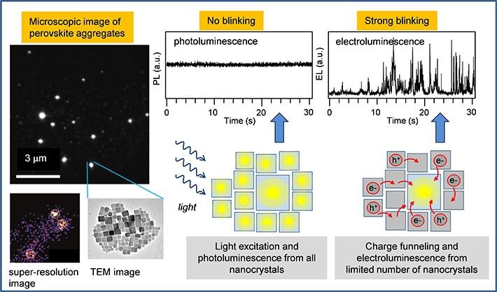
The team used nanocrystals of the perovskite CsPbBr3 surface-passivated with oleic acid ligands, dispersed in thin film of a conducting polymer which was used as an emission layer in a light-emitting device (LED). The device was constructed for use on top of an inverted fluorescence microscope which enabled comparison of electroluminescence and photoluminescence from the same nanocrystals. The CsPbBr3 nanocrystals form aggregates within the emission layer, with each aggregate containing tens to hundreds of individual nanocrystals. The researchers used an advanced microscopic technique of super-resolution imaging to find out that while in photoluminescence all the nanocrystals in the aggregate emit light, in electroluminescence only a small number (typically 3-7) of the nanocrystals are actively emitting (Fig. 1). The electroluminescence from only a limited number of nanocrystals is a result of size distribution and the consequent energy landscape within the aggregate. Electrical charges which are injected into the device during the operation are captured on individual nanocrystals and efficiently funneled towards the largest nanocrystals. The largest nanocrystals within the aggregate have the smallest energy bandgap, and their valence and conduction bands work as traps for charges captured originally at the surrounding nanocrystals. The conductive environment present between the nanocrystals enables efficient migration of the charges to these traps from where the electroluminescence takes place, as shown schematically in Fig. 1.
Another important finding is that the intensity of electroluminescence from the actively emitting nanocrystals is not constant but rather shows strong fluctuations, so called blinking (Fig. 1). Such blinking is not present in photoluminescence of the same aggregates. The researchers have previously found that the blinking can be caused by the conductive matrix as well as by externally applied electric field (ACS Nano13, 2019, 624). In the LED device, the blinking phenomenon is a crucial factor that contributes to the lower efficiency in electroluminescence. The researchers concluded that electroluminescence efficiency is only about one third of that of photoluminescence due to the presence of the blinking phenomenon.
The present work points a way towards efficient nanoscale characterization of electroluminescence of halide perovskite materials for light-emitting applications. One of the keys towards higher efficiency will be surface engineering of the nanocrystals that would suppress the intensity fluctuations.
###
Media Contact
Kazuhide Hasegawa
[email protected]
81-357-342-975
Original Source
https:/
Related Journal Article
http://dx.


