Credit: NASA/Theresa Johnson
NASA astrophysicists and engineers are adapting detectors used by earthbound supercolliders and creating them the same way electronics companies produce all modern consumer devices, including cell phones and laptops.
The new pixel-based silicon detector technology could be used on next-generation gamma-ray observatories to detect highly energetic photons emanating from the most powerful events in the universe, including colliding galaxies and black holes. The new detectors would sense these photons much like a digital camera and use far less power than current space-based detectors.
Underground supercolliders, which have experiments employing the same silicon pixel-type detectors, accelerate protons and ions to near the speed of light in opposite directions at very high energies. Their collisions are designed to recreate the conditions that governed the universe after the Big Bang. Although highly efficient, current silicon pixel technology requires a lot of power, which would be a challenge if used in space where power is normally derived from solar panels.
Enter AstroPix
“The challenge is finding the best way to reduce the amount of power the pixel needs to use since instruments on the ground have access to all the power they want,” said Regina Caputo, an astrophysicist at NASA’s Goddard Space Flight Center in Greenbelt, Maryland, and a fellow with NASA’s Nancy Grace Roman Technology Fellowship program. She is the principal investigator of Goddard’s detector-development effort called AstroPix.
Caputo and her team, which includes Goddard astrophysicist Jeremy Perkins and postbaccalaureate researcher Isabella Brewer, initially began their work with support from Goddard’s Internal Research and Development (IRAD) program. The team has since secured technology-development support from NASA’s Astrophysics Research and Analysis (APRA) program.
Like the particle physics community, Caputo is experimenting with a manufacturing process called complementary metal oxide semiconductor, or CMOS, which NASA’s Jet Propulsion Laboratory finessed for spaceflight applications. The semiconductor industry uses this technique to make modern electronic devices. “This process allows us to not only collect energy from particles that enter the detector, but also to amplify their signals all in the same detector material. This makes these detectors less expensive and noisy,” Caputo said.
With the APRA award, Caputo and her team are designing new pixel detectors optimized for potential use in space. They have sent their first version of AstroPix to a semiconductor foundry — the same facilities that manufacture computer chips — for fabrication.
“We hope to get AstroPix back this summer for testing,” she said. “This is progress.”
Detector Advantages
AstroPix’s advantage is best illustrated by comparing it with detectors flying on the Fermi Gamma-ray Space Telescope. Fermi also uses silicon-based detectors, but its sensors are comprised of silicon strips that are assembled in layers. These layers cross one another perpendicularly to create a grid that pinpoints the locations of high-energy particles created when a gamma ray hits a detector.
With AstroPix, however, particles would be recorded once they contacted a single pixel instead of silicon strip layers, giving the detector the ability to create a map of the particles’ paths with fewer layers.
“Previous silicon strip-detecting technology went through a series of processes to convert charges to digital signals, while the new pixel-based technology can do all of them at once since the readout is integrated with each pixel, Caputo said. In this way, the pixel detector would reduce its power needs to function the best in space.
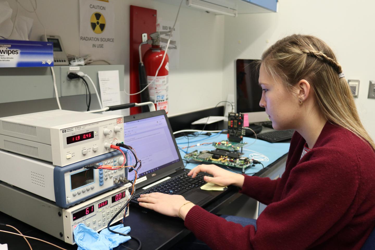
The team is testing the pixel detector in the astrophysics lab at Goddard using radioactive sources, such as cadmium, for the pixelated silicon to detect. The tests help determine whether the energy resolution of the pixel detector is the same or better than the silicon strip detectors. “These sources can partially reproduce the types of radiation found in space, although at a much lower dose,” Brewer said.
If Proven, Future Missions May Benefit
The AstroPiX team must prove the effectiveness of these silicon pixel detectors before the technology could be incorporated into a future gamma-ray mission, Perkins said. In fact, in addition to improved position sensitivity, energy resolution, and lower power consumption, the pixel detector technology would easily be the best choice for any particle-detecting mission because they are easy to produce and inexpensive, especially compared with silicon strip detectors.
###
For more news about Goddard technology, go to: https:/
By Theresa Johnson and Lori Keesey
NASA’s Goddard Space Flight Center, Greenbelt, Maryland
Media Contact
Lori Keesey
[email protected]
Original Source
https:/


