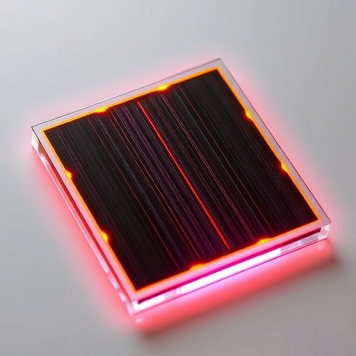
In the quest for more efficient and scalable solar energy solutions, perovskite solar cells (PSCs) have emerged at the forefront of photovoltaic research. Traditional PSCs, characterized by a stacking architecture where the electron-transport layer (ETL) lies beneath the perovskite absorber and the hole-transport layer (HTL) resides atop, have shown commendable performance. Nevertheless, this configuration poses considerable challenges in terms of large-scale manufacturing and operational stability, impeding their commercial viability. Intriguingly, inverted PSCs—which invert the positions of the ETL and HTL—have gained momentum due to their promising power conversion efficiency and enhanced compatibility with scalable, solution-based fabrication methods. These attributes highlight inverted PSCs as a transformative avenue for next-generation solar technology.
Yet, the advancement of inverted PSCs has been hindered by persistent issues at the microscopic level. Chief among these challenges is the poorly regulated buried interface—the critical boundary where the perovskite active layer contacts the hole-transport layer. This interface suffers from uncontrolled microstructures and the presence of electronic defects, which collectively degrade device performance and undermine long-term operational stability. Addressing these interface-related problems is essential for unlocking the full potential of inverted PSCs.
Researchers from the Qingdao Institute of Bioenergy and Bioprocess Technology (QIBEBT) under the Chinese Academy of Sciences have pioneered an innovative crystal-solvate (CSV) pre-seeding methodology that precisely engineers this elusive buried interface. Their breakthrough approach enables unprecedented control over the bottom interface’s morphology and electronic characteristics, thereby facilitating the creation of high-efficiency, large-area perovskite photovoltaic modules. This seminal study was recently disclosed in the prestigious journal Nature Synthesis, marking a significant milestone in photovoltaic materials science.
The cornerstone of the team’s technique is the deliberate pre-deposition of low-dimensional halide crystal-solvate seeds, chemically denoted as PDPbI₄·DMSO, onto substrates modified with self-assembled monolayers (SAMs). These CSV nanocrystals serve as a meticulously designed structural scaffold that templates the crystallization of the succeeding perovskite layer. Their unique rod-shaped, anisotropic morphology significantly refines the wettability of the naturally hydrophobic SAM surface, ensuring the homogeneous spreading of the perovskite precursor solution. This modulation of surface energy is a critical enabler for uniform film formation, which is fundamental to device reproducibility and performance.
More profoundly, during the nucleation and growth phases of the perovskite film, these pre-seeded CSV nanocrystals act as abundant heterogeneous nucleation centers. This nucleation density enhancement expedites perovskite crystallization kinetics, producing a more consistent and ordered polycrystalline structure. Such finely tuned crystallization dynamics mitigate defect generation and grain boundary irregularities, which are notorious for impairing charge transport and accelerating device degradation.
A particularly novel aspect of this strategy lies in the entrapment of dimethyl sulfoxide (DMSO) solvent molecules within the CSV crystalline lattice. Upon thermal annealing—a critical post-deposition process—these solvent molecules are gradually liberated in a spatially confined, bottom-interface microenvironment. This creates a transformative “lattice-confined solvent annealing” effect, wherein the controlled release of solvent vapors promotes grain reorganization and growth selectively at the interface without compromising the integrity of the entire perovskite layer. This gentle solvent atmosphere works synergistically with the seed-induced crystallization, culminating in a robust, defect-suppressed grain architecture.
The integrated control of crystallization and interfacial stabilization manifests dramatically in the film morphology. The CSV pre-seeding approach effectively eliminates interfacial voids and smooths grain boundary grooves, which are typical sites of electronic traps and recombination centers. The resulting perovskite “bottom layer” is densely packed and highly oriented, exhibiting significantly enhanced electronic properties and superior photothermal stability. These improvements directly translate into better charge carrier mobility, prolonged operational lifespan, and minimized performance deterioration under real-world conditions.
To bridge the gap between laboratory-scale innovation and practical manufacturing, the research team incorporated the CSV pre-seeding method into a slot-die coating process, a scalable and industry-relevant technique. This hybrid manufacturing approach enabled the fabrication of a perovskite solar mini-module with an active aperture area of nearly 50 cm²—a size relevant for commercial application. Remarkably, this mini-module achieved a power conversion efficiency (PCE) of 23.15%, with a negligible efficiency loss of less than 3% compared to smaller-area cells. Such scaling performance retention outpaces many previously reported perovskite photovoltaic systems and is pivotal for real-world deployment.
Professor Pang Shuping, a leading figure in this research, underscored the significance of overcoming the longstanding scaling bottleneck attributed to size effects by harmonizing induced crystallization with buried interface restoration. Beyond the immediate application to perovskite photovoltaics, this crystal-solvate pre-seeding paradigm represents a versatile materials platform. By tuning the organic cations and solvent molecules comprising the CSV seeds, an extensive library of bespoke CSV compounds can be crafted. This tunability paves the way for customizable interface engineering strategies tailored for a broad spectrum of soft-lattice semiconductors and optoelectronic devices beyond solar cells.
This pioneering work redefines the roadmap for interface engineering by demonstrating that precision crystal nucleation control combined with controlled interfacial solvent modulation can surmount previously intractable barriers to device efficiency and stability. The implication is clear: such molecular-level design and process integration will propel perovskite photovoltaic technologies closer to commercial realization, while simultaneously expanding the foundational understanding of crystal growth mechanisms in complex thin-film systems.
As solar energy continues to assume a central role in global renewable energy portfolios, innovations like the CSV pre-seeding method promise to drive the next generation of high-performance, scalable photovoltaic technologies. The amalgamation of fundamental materials chemistry with applied device engineering showcased in this study represents a beacon of progress, illuminating pathways toward cleaner, more sustainable energy futures.
Subject of Research: Advancement of buried interface engineering in inverted perovskite solar cells through crystal-solvate pre-seeding for enhanced crystallization and stability.
Article Title: Crystal-Solvate Pre-Seeding Strategy Enables Precise Buried Interface Regulation for High-Efficiency, Scalable Inverted Perovskite Solar Cells
News Publication Date: February 27, 2026
Web References:
http://dx.doi.org/10.1038/s44160-026-00993-x
Image Credits: Image by SUN Xiuhong, Qingdao Institute of Bioenergy and Bioprocess Technology, Chinese Academy of Sciences
Keywords
Perovskite Solar Cells, Crystal-Solvate Pre-Seeding, Buried Interface, Inverted PSC, Crystallization Control, Photovoltaics, Interface Engineering, Dimethyl Sulfoxide, Thermal Annealing, Slot-Die Coating, Power Conversion Efficiency, Large-Area Solar Modules
Tags: buried interface defects in inverted PSCselectron-transport layer and hole-transport layer interfaceenhancing operational stability of perovskite solar cellsinterface engineering in solar cellsinverted perovskite solar cells performancelarge-scale manufacturing of inverted perovskite solar cellsmicrostructure control in perovskite solar cellsnext-generation photovoltaic technologypower conversion efficiency improvement in PSCsQingdao Institute bioenergy solar researchscalable solution-based perovskite solar cell fabrication


