A team of scientists led by ITMO researchers proposed a quick and affordable method to create optical chips right in a Petri dish. The research was published in ACS Nano.
Credit: Article’s authors
The modern photonics industry is constantly working on making its devices more compact, be it computing systems or sensors and lidars. For this, it is necessary to make lasers, transistors and other elements smaller. A team of scientists led by ITMO researchers proposed a quick and affordable method to create optical chips right in a Petri dish. The research was published in ACS Nano.
Nowadays, using devices that are based on microscopic lasers and optical chips is becoming more and more common. They are used in the production of lidars, in the development of new biosensors, and in the future, they can become the foundation for new optical computers that will use photons rather than electrons to transfer and process information. Today’s optical chips operate in the infrared (IR) range, i.e. the lasers they use emit at the wavelengths that’s invisible to the human eye.
“But to make the devices even more compact, we need to work in the visible range,” says Sergey Makarov, chief researcher at ITMO’s Department of Physics and Engineering, “as the size of a chip depends on the wavelength of its emission.”
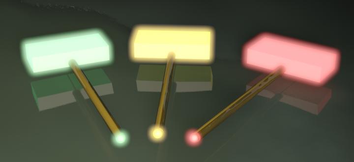
An optical chip consists of such components as lasers and waveguides. While creating a source that would emit in the green or red part of the spectrum is quite easy, waveguides for these wavelengths can be an issue.
“A microlaser is a source of emission that you need to guide somewhere,” comments Ivan Sinev, senior researcher at ITMO’s Department of Physics and Engineering, “and this is what waveguides are for. But the standard silicon waveguides that are used in IR optics do not work in the visible range. They transmit the signal no further than several micrometers. For an optical chip, we need to transmit along tens of micrometers with a high localization, so that the waveguide would have a very small diameter and the light would go sufficiently far through it.”
Scientists made attempts to replace silicon waveguides with silver ones, but the transmission distance in such systems was also insufficient. In the end, a team of scientists that included specialists from ITMO University used gallium phosphide as a material for the waveguides, as it has very low losses in the visible band. But the most important thing is that both the light source can be grown directly on a waveguide in a Petri dish using solution chemistry methods, which is way cheaper than the commonly used nanolithography.
The size of the new chip’s elements is about three times smaller than that of its counterparts that work in the IR spectral range.
“The chip’s important property is its ability to tune the emission color from green to red by using a very simple procedure: an anionic exchange between perovskite and hydrogen halides vapor,” notes Anatoly Pushkarev, senior researcher at ITMO’s Department of Physics and Engineering. “Importantly, you can change the emission color after the chip’s production, and this process is reversible. This could be useful for the devices that have to transmit many optical signals at different wavelengths. For example, you can create several lasers for such a device, connect them to a single waveguide, and use it for transmitting several signals of different colors at once.”
The scientists also equipped the newly created chip with an optical nanoantenna made of perovskite that receives the signal travelling along the waveguide and allows uniting two chips in a single system.
“We added a nanoantenna at the other end of our waveguide,” explains Pavel Trofimov, PhD student at ITMO’s Department of Physics and Engineering, “so now we have a light source, a waveguide, and a nanoantenna that emits light when pumped by the microlaser’s emission. We added another waveguide to it: as a result, the emission from a single laser went into two waveguides. At the same time, the nanoantenna did not just connect these elements into a single system, but also converted part of the green light into the red spectrum.”
###
Media Contact
Alena Gupaisova
[email protected]
Related Journal Article
http://dx.


