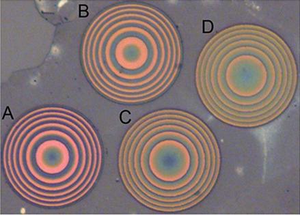

Credit: Liu et al., Nano Letters, 2018
November 13, 2018
In optics, the era of glass lenses may be waning.
In recent years, physicists and engineers have been designing, constructing and testing different types of ultrathin materials that could replace the thick glass lenses used today in cameras and imaging systems. Critically, these engineered lenses — known as metalenses — are not made of glass. Instead, they consist of materials constructed at the nanoscale into arrays of columns or fin-like structures. These formations can interact with incoming light, directing it toward a single focal point for imaging purposes.
But even though metalenses are much thinner than glass lenses, they still rely on "high aspect ratio" structures, in which the column or fin-like structures are much taller than they are wide, making them prone to collapsing and falling over. Furthermore, these structures have always been near the wavelength of light they're interacting with in thickness — until now.
In a paper published Oct. 8 in the journal Nano Letters, a team from the University of Washington and the National Tsing Hua University in Taiwan announced that it has constructed functional metalenses that are one-tenth to one-half the thickness of the wavelengths of light that they focus. Their metalenses, which were constructed out of layered 2D materials, were as thin as 190 nanometers — less than 1/100,000ths of an inch thick.
"This is the first time that someone has shown that it is possible to create a metalens out of 2D materials," said senior and co-corresponding author Arka Majumdar, a UW assistant professor of physics and of electrical and computer engineering.
Their design principles can be used for the creation of metalenses with more complex, tunable features, added Majumdar, who is also a faculty researcher with the UW's Molecular Engineering & Sciences Institute.
Majumdar's team has been studying the design principles of metalenses for years, and previously constructed metalenses for full-color imaging. But the challenge in this project was to overcome an inherent design limitation in metalenses: in order for a metalens material to interact with light and achieve optimal imaging quality, the material had to be roughly the same thickness as the light's wavelength in that material. In mathematical terms, this restriction ensures that a full zero to two-pi phase shift range is achievable, which guarantees that any optical element can be designed. For example, a metalens for a 500-nanometer lightwave — which in the visual spectrum is green light — would need to be about 500 nanometers in thickness, though this thickness can decrease as the refractive index of the material increases.
Majumdar and his team were able to synthesize functional metalenses that were much thinner than this theoretical limit — one-tenth to one-half the wavelength. First, they constructed the metalens out of sheets of layered 2D materials. The team used widely studied 2D materials such as hexagonal boron nitride and molybdenum disulfide. A single atomic layer of these materials provides a very small phase shift, unsuitable for efficient lensing. So the team used multiple layers to increase the thickness, although the thickness remained too small to reach a full two-pi phase shift.
"We had to start by figuring out what type of design would yield the best performance given the incomplete phase," said co-author Jiajiu Zheng, a doctoral student in electrical and computer engineering.
To make up for the shortfall, the team employed mathematical models that were originally formulated for liquid-crystal optics. These, in conjunction with the metalens structural elements, allowed the researchers to achieve high efficiency even if the whole phase shift is not covered. They tested the metalens' efficacy by using it to capture different test images, including of the Mona Lisa and a block letter W. The team also demonstrated how stretching the metalens could tune the focal length of the lens.
In addition to achieving a wholly new approach to metalens design at record-thin levels, the team believes that its experiments show the promise of making new devices for imaging and optics entirely out of 2D materials.
"These results open up an entirely new platform for studying the properties of 2D materials, as well as constructing fully functional nanophotonic devices made entirely from these materials," said Majumdar.
Additionally, these materials can be easily transferred on any substrate, including flexible materials, paving a way towards flexible photonics.
###
The lead and co-corresponding author on the paper is Chang-Hua Liu, who began this work as a UW postdoctoral researcher and is now a faculty member at the National Tsing Hua University in Taiwan. Additional co-authors are doctoral students Shane Colburn, Taylor Fryett and Yueyang Chen in the Department of Electrical and Computer Engineering; and Xiaodong Xu, a UW professor of physics and of materials science and engineering. The team's prototype metalenses were all built at the Washington Nanofabrication Facility on the UW campus. The research was funded by the U.S. Air Force Office of Scientific Research, the National Science Foundation, the Washington Research Foundation, the M.J. Murdock Charitable Trust, GCE Market, Class One Technologies and Google.
For more information, contact Majumdar at [email protected]">[email protected].
Grant numbers: FA9550-18-1-0104, 1719797, 0335765, 1337840
Link to full release with images: http://www.washington.edu/news/2018/11/13/metalens-2d-materials/
Media Contact
James Urton
[email protected]
206-543-2580
@UW
http://www.washington.edu/news/
Original Source
http://www.washington.edu/news/2018/11/13/metalens-2d-materials/ http://dx.doi.org/10.1021/acs.nanolett.8b02875


