A model of temperature dependence of dislocation-related photoluminescence in ion-doped silicon has been proposed for the first time. Calculations using this model explain the increased temperature stability of photoluminescence found in experiments.
Credit: Lobachevsky University
Silicon is the main material in electronic engineering. All information and computing technologies that play a key role in modern civilization are based on silicon: computers, communications, astronautics, biomedicine, robotics and much more.
According to Alexey Mikhaylov, Head of the laboratory at the Lobachevsky University’s Research Institute for Physics and Technology, the main stumbling block on the way to increasing the speed of integrated circuits is the limited speed of electrical signal propagation in metal interconnection wiring. “This requires the replacement of metal interconnections with optical waveguides and, thus, the transition from traditional electronics to optoelectronics, where the active elements are light emitters and receivers rather than transistors”, says Alexey Mikhaylov.
Silicon shows satisfactory performance as light receiver, but, unlike A3B5 semiconductors, is a poor light emitter because of an indirect bandgap of this semiconductor. This feature of its electronic structure, according to the laws of quantum mechanics, strictly speaking, prohibits the emission of light (luminescence) under external excitation.
“It would be very undesirable to refuse from silicon at a new stage, as we would have to abandon the perfectly developed technology for mass production of integrated circuits. This would involve huge material costs, not to mention the environmental problems that arise when working with A3B5 materials,” states Professor David Tetelbaum, Leading Researcher at Lobachevsky University.
Scientists are trying to find a way out of this situation by either using nanocrystalline silicon, or by coating silicon with films of other light-emitting materials. However, the emissivity (luminescence efficiency) of silicon nanocrystals is still insufficient for practical applications.
Besides, silicon nanocrystals emit in the area at the “red” edge of visible radiation, while many technical applications, in particular in fiber optics communication technology, require longer wavelengths (about 1.5 μm). The use of “foreign” material layers on silicon substrates, however, is poorly compatible with the traditional silicon technology.
An effective way to solve this problem is to introduce in silicon a special type of linear defects known as dislocations. Researchers have come to the conclusion that a high concentration of dislocations can be achieved in the silicon surface layer by irradiating it with silicon ions with the energy of the order of a hundred keV and then annealing it at high temperatures. In this case, silicon emits light at exactly the right wavelength – close to 1.5 μm.
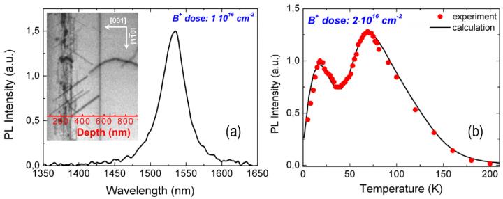
“The luminescence intensity appears to depend on the implantation and annealing conditions. However, the main problem with dislocation-related luminescence is that it is most pronounced at low temperatures (below ~25 K) and decays quickly as the temperature rises. Therefore, it is very important to find ways to increase the thermal stability of dislocation-related luminescence”, continues Alexey Mikhaylov.
Lobachevsky University scientists together with their colleagues from the RAS Institute of Solid State Physics (Chernogolovka) and the Alekseev State Technical University (Nizhny Novgorod) have made significant headway in solving this problem with the support of the Russian Foundation for Basic Research (grant No.17-02-01070).
Previously, it was found that one way to achieve dislocation-related photoluminescence in silicon samples is to implant silicon ions into silicon (self-implantation) with subsequent annealing. This proved to be not the only benefit of the implantation technology, when the team of Lobachevsky University discovered that additional boron ion doping can enhance the luminescence. However, the phenomenon of enhanced luminescence properties alone does not solve the main problem. Moreover, it remained unclear how boron ion doping affects the luminescence thermal stability, which is a key parameter, and under what conditions (if any) such effect will be most pronounced.
In this study, scientists have confirmed experimentally the increase in thermal stability of silicon doped with boron ions. Moreover, the effect is nonmonotonically dependent on the boron dose, and in a certain range of doses, a pronounced second maximum in the region of 90 to 100 K appears on the intensity versus temperature curve, along with the usual low-temperature maximum in the region of 20 K.
“It is important to note that the “beneficial” effect of boron is unique in the sense that the replacement of boron ions by another acceptor impurity does not lead to the effect described above. After refining the modes of boron ion doping and heat treatment of silicon samples where centers of dislocation-related luminescence were formed by irradiation with silicon ions, we have found that with the highest previously used dose of boron ions and an additional heat treatment at 830° C, it is possible to achieve a measurable level of luminescence at room temperature,” concludes Professor Tetelbaum.
The results obtained during further optimization of the implantation and heat treatment conditions brighten up the prospects for silicon application in optoelectronics.
###
An article on the results of this work was recently published in the authoritative journal Nuclear Instruments and Methods in Physics Research B: Beam Interactions with Materials and Atoms.
Media Contact
Alexey Pomazov
[email protected]
Related Journal Article
http://dx.


