
As the demand for more compact and efficient electronic devices rises, researchers have increasingly focused on enhancing the materials used in computer chips. One major stumbling block in this pursuit has been the limitations of conventional metal conductors, particularly copper, as they are scaled down. A recent study from Stanford University reveals an exciting development in this realm: niobium phosphide (NbP), a topological semimetal, showcases superior electrical conductivity properties even at extremely thin dimensions. This breakthrough is set to revolutionize the way we approach nanoscale electronics.
Niobium phosphide differs fundamentally in its structure and electrical properties when compared to traditional conductors. As computer chips shrink, the wires they utilize also undergo downsizing. However, as these wires diminish in width, their ability to conduct electricity diminishes as well, resulting in increased resistance and heat generation. Researchers have concluded that copper becomes inefficient and loses conductivity at thicknesses of less than 50 nanometers. In stark contrast, the findings concerning niobium phosphide demonstrate that it maintains superior conductivity at sizes down to just 5 nanometers.
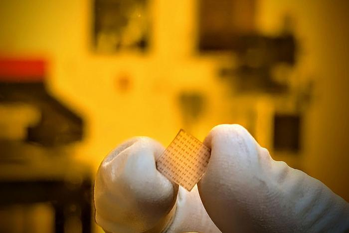
The team led by researcher Asir Intisar Khan has invented a process to create and deposit niobium phosphide films at achievable temperatures that do not compromise the silicon chips they would be used on. This is critical for the scalable manufacturing of future electronic devices, as it addresses the high-temperature limitations of creating lattice-perfect materials. Niobium phosphide’s capacity to be deposited under accessible conditions propels it ahead as a candidate for integration into existing manufacturing processes without the need for extensive redesign of fabrication techniques.
The semiconductor industry has long been on the lookout for alternative materials to copper, particularly in light of the pressing demands for faster transfer speeds and higher efficiency in data processing. The transition to ultrathin films of niobium phosphide offers the intriguing possibility of overcoming some of the fundamental limits imposed by traditional metals. Moreover, this material not only proves to be more efficient at room temperature, but it also lessens the amount of energy lost to heating — a critical factor that can cumulatively lead to significant energy savings, especially when scaled across hundreds or thousands of chips in data centers.
As niobium phosphide is classified as a topological semimetal, its unique surface contributions to conductivity become increasingly vital as the material is thinned. Conventional metals have a relatively uniform conductive profile, but niobium phosphide manages to thrive on its surface attributes as it is reduced in size. This separation of conduction pathways allows for heightened efficiency, making copper, which deteriorates beyond a certain thickness, potentially obsolete for specific nanoscale applications.
In an era where data centers are consuming more energy than ever before, optimizing the connection materials used in processors could lead to reduced electricity costs and smaller carbon footprints. Khan pointed out that even minor enhancements in efficiency could accrue substantial benefits when applied to large-scale electronic infrastructures, which often utilize thousands of chips simultaneously. The goal here is not merely to replace copper, which still performs admirably at larger scales, but to usher in materials that excel in the increasingly fine connections that contemporary technology demands.
The development of niobium phosphide films stands out for enabling the flexibility necessary in electronic material design. Previous attempts to substitute copper with more advanced materials often necessitated precise crystalline structures established at extremely high temperatures, thus complicating integration into traditional semiconductor processes. The research team’s ability to create non-crystalline films marks a watershed moment in semiconductor technology, enabling new configurations that were previously deemed unfeasible.
Prominent research figures, including co-author Akash Ramdas, emphasized that the real-world applicability of these materials is crucial for their eventual adoption in consumer electronics. The transition from theoretical science to practical tools in electrical engineering requires extensive testing and validation. For this reason, Khan and his colleagues are diligently working on transforming their thin films into narrow wires, setting the stage for real-world testing that could help solidify the role of niobium phosphide in future technology.
Moreover, the collaborative nature of this research demonstrates the shared focus across the academic community to innovate in materials engineering. This collective endeavor is designed to overcome existing hurdles in conductor applications, as highlighted by senior authors such as Eric Pop, who emphasizes the need for efficient signal processing in high-density electronics. As they explore additional topological semimetals, there is an eagerness to comprehend how these materials can address the mounting demands of modern computing without introducing excessive cost or complexity.
In summary, niobium phosphide emerges as a groundbreaking contender in the landscape of electronics, with the potential to redefine standards for conductivity and efficiency in future devices. As they continue to investigate this novel class of materials, the researchers remain optimistic about the implications of their work, which may very well reshape the trajectory of electronic design in the coming years. The pursuit of effective and reliable materials like niobium phosphide marks a critical step in ensuring that ever-smaller devices continue to meet the intensifying demands for speed and energy efficiency.
With further exploration and research, niobium phosphide could lead to expansive advancements in energy conservation, sustainability in technology, and a rethinking of how we engineer the chips that power our digital world. The path to new technological frontiers is paved with innovative material science, and niobium phosphide is at the forefront of this quest.
Subject of Research: Niobium phosphide films for advanced electronic applications
Article Title: Surface conduction and reduced electrical resistivity in ultrathin noncrystalline NbP semimetal
News Publication Date: 3-Jan-2025
Web References: DOI Link
References: The research team from Stanford University and related institutions
Image Credits: Asir Khan / Eric Pop
Keywords
Electrical conductors, Alternative energy, Thermal energy, Computer science, Integrated circuits, Thin film deposition


