
Credit: Mikko Raskinen / Aalto University
Ionotronic devices rely on charge effects based on ions, instead of electrons or in addition to electrons. These devices open new opportunities for creating electrically switchable memories. However, there are still many technical challenges to overcome before this new kind of memories can be produced.
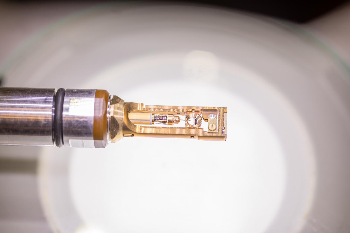
Researchers at Aalto University in Finland have visualized how oxygen ion migration in a complex oxide material causes the material to alter its crystal structure in a uniform and reversible fashion, prompting large modulations of electrical resistance. They performed simultaneous imaging and resistance measurements in a transmission electron microscope using a sample holder with a nanoscale electrical probe. Resistance-switching random access memories could utilize this effect.
Sample holder helps control migration of ions
"In a transmission electron microscope, a beam of high-energy electrons is transmitted through a very thin specimen. Various detectors collect the electrons after their interaction with the sample, providing detailed information about the atomic structure and composition of the material. The technique is extremely powerful for nanomaterials characterization, but if used conventionally, it does not allow for active material manipulation inside the microscope. In our study, we utilized a special sample holder with a piezo-controlled metallic probe to make an electrical nanocontact. This in situ method allowed us to apply short voltage pulses and thereby control the migration of oxygen ions in our sample," explains Academy of Finland Research Fellow Lide Yao.
The researchers found that migration of oxygen ions away from the contact area results in an abrupt change in the oxide lattice structure and an increase of electrical resistance. Reversal of the voltage polarity fully restores the original material properties. Electro-thermal simulations, performed by PhD candidate Sampo Inkinen, showed that a combination of current-induced sample heating and electric-field-directed ion migration causes the switching effect.
Ionotronic concept for manipulation of several material properties
"The material that we investigated in this study is a complex oxide. Complex oxides can exhibit many interesting physical properties including magnetism, ferroelectricity, and superconductivity, and all these properties vary sensitively with the oxidation state of the material. Voltage-induced migration of oxygen ions does change the amount of oxidation, triggering strong material responses. While we have demonstrated direct correlations between oxygen content, crystal structure, and electrical resistance, the same ionotronic concept could be utilized to control other material properties," says Professor Sebastiaan van Dijken, who is a coauthor on the paper with Yao.
"In the current study, we employed a special sample holder for simultaneous measurements of the atomic-scale structure and electrical resistance. We are now developing an entirely new and unique holder that would allow for transmission electron microscopy measurements while the specimen is irradiated by intense light. We plan to investigate atomic scale processes in perovskite solar cells and other optoelectronic materials with this setup in the future," adds Yao.
###
Nature Communications published the results this week. The in situ transmission electron microscopy study was performed at the Aalto's Nanomicroscopy Center for high-resolution material characterization and part of Finland's national research infrastructure, OtaNano.
Media Contact
Lide Yao
[email protected]
358-503-443-612
@aaltouniversity
http://www.aalto.fi/en/
############
Story Source: Materials provided by Scienmag

