‘Honey, I shrunk the detector’
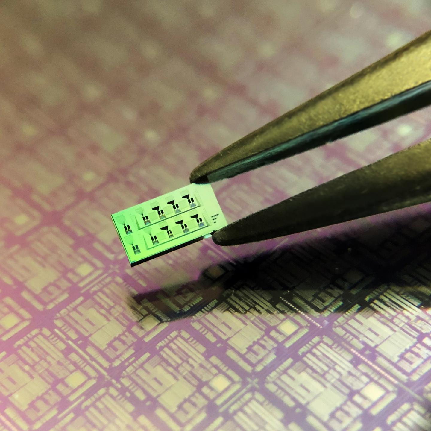
Credit: © Helmholtz Zentrum Muenchen / Roman Shnaiderman
Researchers at Helmholtz Zentrum München and the Technical University of Munich (TUM) have developed the world’s smallest ultrasound detector. It is based on miniaturized photonic circuits on top of a silicon chip. With a size 100 times smaller than an average human hair, the new detector can visualize features that are much smaller than previously possible, leading to what is known as super-resolution imaging.
Since the development of medical ultrasound imaging in the 1950s, the core detection technology of ultrasound waves has primarily focused on using piezoelectric detectors, which convert the pressure from ultrasound waves into electric voltage. The imaging resolution achieved with ultrasound depends on the size of the piezoelectric detector employed. Reducing this size leads to higher resolution and can offer smaller, densely packed one or two dimensional ultrasound arrays with improved ability to discriminate features in the imaged tissue or material. However, further reducing the size of piezoelectric detectors impairs their sensitivity dramatically, making them unusable for practical application.
Using computer chip technology to create an optical ultrasound detector
Silicon photonics technology is widely used to miniaturize optical components and densely pack them on the small surface of a silicon chip. While silicon does not exhibit any piezoelectricity, its ability to confine light in dimensions smaller than the optical wavelength has already been widely exploited for the development of miniaturized photonic circuits.
Researchers at Helmholtz Zentrum Mu?nchen and TUM capitalized on the advantages of those miniaturized photonic circuits and built the world’s smallest ultrasound detector: the silicon waveguide-etalon detector, or SWED. Instead of recording voltage from piezoelectric crystals, SWED monitors changes in light intensity propagating through the miniaturized photonic circuits.
“This is the first time that a detector smaller than the size of a blood cell is used to detect ultrasound using the silicon photonics technology”, says Rami Shnaiderman, developer of SWED. “If a piezoelectric detector was miniaturized to the scale of SWED, it would be 100 million times less sensitive.”
Super-resolution imaging
“The degree to which we were we able to miniaturize the new detector while retaining high sensitivity due to the use of silicon photonics was breathtaking”, says Prof. Vasilis Ntziachristos, lead of the research team. The SWED size is about half a micron (=0,0005 millimeters). This size corresponds to an area that is at least 10,000 times smaller than the smallest piezoelectric detectors employed in clinical imaging applications. The SWED is also up to 200 times smaller than the ultrasound wavelength employed, which means that it can be used to visualize features that are smaller than one micrometer, leading to what is called super-resolution imaging.
Inexpensive and powerful
As the technology capitalizes on the robustness and easy manufacturability of the silicon platform, large numbers of detectors can be produced at a small fraction of the cost of piezoelectric detectors, making mass production feasible. This is important for developing a number of different detection applications based on ultrasound waves. “We will continue to optimize every parameter of this technology – the sensitivity, the integration of SWED in large arrays, and its implementation in hand-held devices and endoscopes”, adds Shnaiderman.
Future development and applications
“The detector was originally developed to propel the performance of optoacoustic imaging, which is a major focus of our research at Helmholtz Zentrum München and TUM. However, we now foresee applications in a broader field of sensing and imaging”, says Ntziachristos.
While the researchers are primarily aiming for applications in clinical diagnostics and basic biomedical research, industrial applications may also benefit from the new technology. The increased imaging resolution may lead to studying ultra-fine details in tissues and materials. A first line of investigation involves super-resolution optoacoustic (photoacoustic) imaging of cells and micro-vasculature in tissues, but the SWED could be also used to study fundamental properties of ultrasonic waves and their interactions with matter on a scale that was not possible before.
###
Collaboration and patenting
The Institute of Biological and Medical Imaging at Helmholtz Zentrum München, the Chair of Biological Imaging at TUM, and TranslaTUM – the Central Institute for Translational Cancer Research at TUM’s university hospital Klinikum Rechts der Isar, have contributed equally to this new technology which was published in the journal Nature. Protection of the intellectual aspects of this technology is ongoing.
Helmholtz Zentrum München
Helmholtz Zentrum München is a research center with a mission to discover personalized medical solutions for the prevention and therapy for environmentally triggered diseases and promote a healthier society in a rapidly changing world. Helmholtz Zentrum München is headquartered in Neuherberg in the north of Munich and has about 2,500 staff members. It is a member of the Helmholtz Association, the largest scientific organization in Germany with more than 40,000 employees at 19 research centers.
Media Contact
Vangelis Papagrigoriou
[email protected]
Related Journal Article
http://dx.


