Credit: by Jun Xing, Chen Zhao, Yuting Zou, Wenchi Kong, Zhi Yu, Yuwei Shan, Qingfeng Dong, Ding Zhou, Weili Yu and Chunlei Guo
Lead halide perovskites can be turned into optoelectronic devices through low-cost solution depositions, but these approaches often leave numerous charge-trapping defects in the perovskite. Continuously improving the performance of these optoelectronic devices is needed to overcome the bottleneck problem. The defect (including surface defects and volume defects) density in perovskites is a key parameter that limits the performance of these materials. To control the surface defects, a widely studied method is to passivate and cure the defects by a surface engineering process, which can be achieved by adding a variety of additives, including ammonium methyl bromide, guanidinium bromide, potassium iodide18, phenethyl iodide, poly(3-hexylthiophene-2,5-diyl), choline iodine, and 1-butyl-3-methylimidazolium tetrafluoroborate. However, this method requires precise control of the amount of the additives, the order of addition, and the reaction time, which makes this process complicated and results in a high risk of loss. To tune the volume defects, a known strategy is irradiating perovskite with high-energy ultraviolet light, sunlight, near-infrared light, etc. This strategy requires a long repair time and sometimes results in irreversible damage to the materials, which makes the process complicated. Therefore, highly efficient and convenient pathways to regulate defects in perovskites are still needed.
In a new paper published in Light Science & Application, the team of scientists, led by Associate Professor Weili Yu, Professor Chunlei Guo from the Photonics Laboratory, State Key Laboratory of Applied Optics, Changchun Institute of Optics, Fine Mechanics and Physics, Chinese Academy of Sciences and Professor Qingfeng Dong from State Key Laboratory of Supramolecular Structure and Materials, Jilin University have jointly developed a technique (voltage regulation engineering) for modifying the defect population of perovskite crystals without requiring chemical additives.
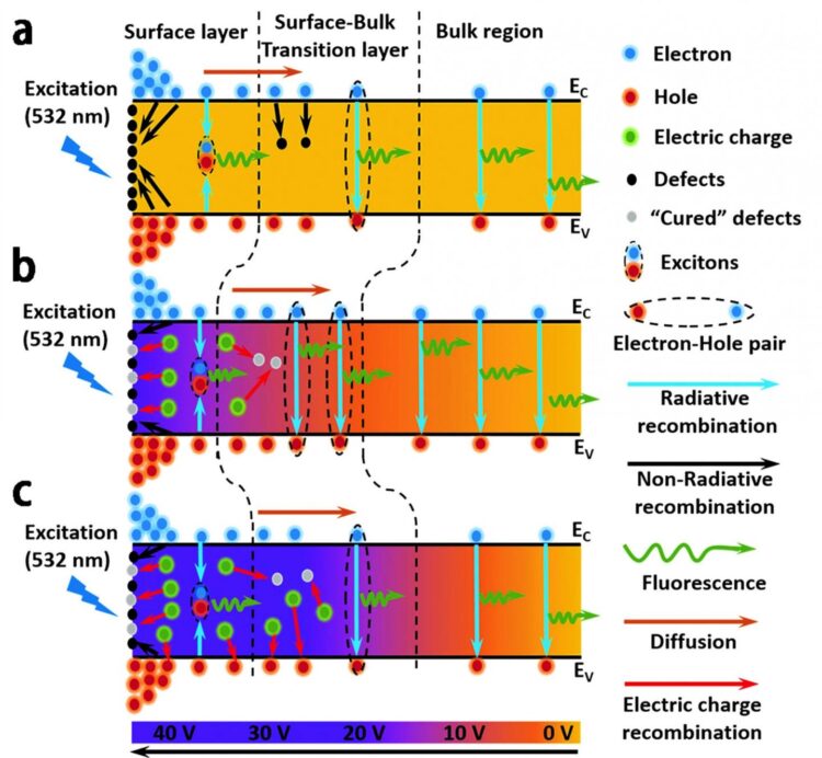
The team used probes to apply an electric field to the surface of a perovskite sample for helping move injected charges into defect sites with a high degree of control, as well as the optical and electrical properties of perovskite sample. Futhermore, the optimized defect populations enabled the perovskite to act as memristor device, capable of activating multiple resistance states.
These scientists summarize the operational principle of the voltage regulation engineering: “The voltage regulation engineering as an efficient strategy can regulate the defects in perovskites and influence its dynamic carrier transport. The injected charges act as a Lewis base can be trapped by lead defects in the surface layer and further passivate the deep-level donor-like defects inside the perovskites. Thus, these “cured” defects no longer trap carriers, and the probability of radiation recombination in perovskites is enhanced, which further improve its optical and electrical properties.”
“This work provides novel insight into the flexibility of the defect density of perovskites, and voltage regulation is an effective engineering method to tune not only the defect density but also the carrier lifetime, PL intensity and resistance. This work will improve the optimization of optoelectronic devices based on perovskites single crystals.” they added and forecast.
###
Media Contact
Weili Yu
[email protected]
Related Journal Article
http://dx.


