• HOME
  • NEWS
  • EXPLORE
    • CAREER
      • Companies
      • Jobs
    • EVENTS
    • iGEM
      • News
      • Team
    • PHOTOS
    • VIDEO
    • WIKI
  • BLOG
  • COMMUNITY
    • FACEBOOK
    • INSTAGRAM
    • TWITTER
Thursday, October 23, 2025
BIOENGINEER.ORG
No Result
View All Result
  • Login
  • HOME
  • NEWS
  • EXPLORE
    • CAREER
      • Companies
      • Jobs
        • Lecturer
        • PhD Studentship
        • Postdoc
        • Research Assistant
    • EVENTS
    • iGEM
      • News
      • Team
    • PHOTOS
    • VIDEO
    • WIKI
  • BLOG
  • COMMUNITY
    • FACEBOOK
    • INSTAGRAM
    • TWITTER
No Result
View All Result
Bioengineer.org
No Result
View All Result
Home NEWS Science News

Reducing down to 1/3 of thermal resistance by WOW technology for 3-D DRAM application

Bioengineer by Bioengineer
April 24, 2017
in Science News
Reading Time: 2 mins read
0
Share on FacebookShare on TwitterShare on LinkedinShare on RedditShare on Telegram
IMAGE

Credit: Tokyo Institute of Technology

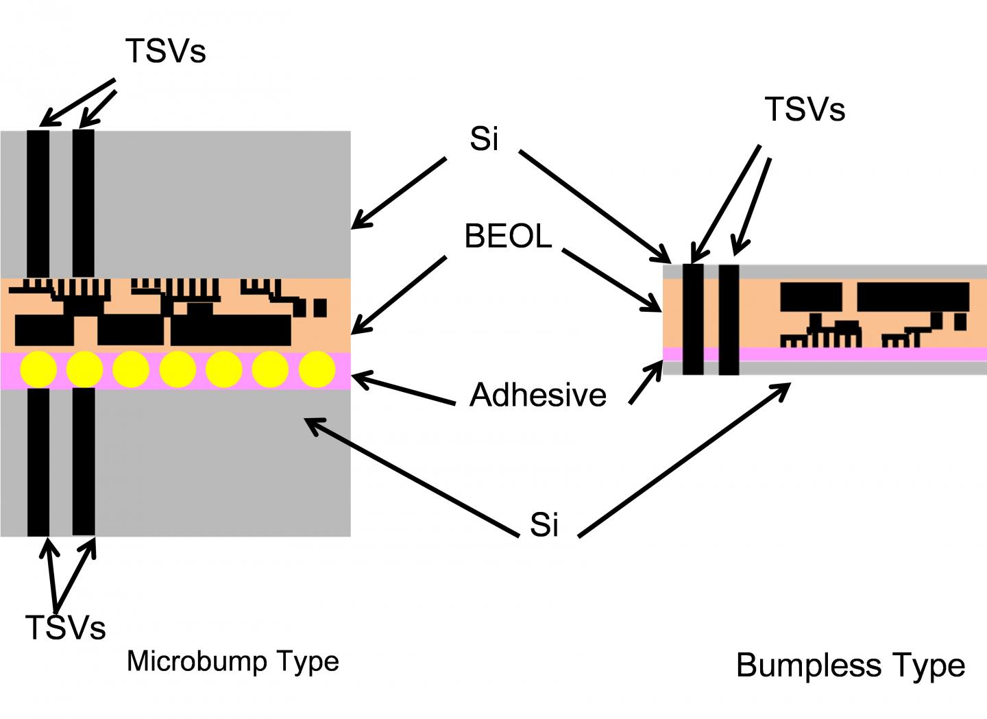
Researcher team led by Professor Takayuki Ohba at Tokyo Institute of Technology, ICE Cube Center, in collaboration with the WOW (Wafer-on-Wafer) Alliance(term 2), an Industry-academic collaborative research organization consisting of multiple semiconductor related companies aiming for practical applications of 3D IC technology, demonstrated the thermal resistance of the 3D stacked device can be reduced down to less than 1/3 relative to the conventional one bonded by bump(term 3) 3D IC in Through-Silicon-Via (TSV) wiring(term 4). Since semiconductor circuits are highly heat-generating bodies during operation, when heat is hard to be released, the temperature of the semiconductor results in highly rise, which leads to be a malfunction. The development of heat dissipation technology has been a big challenge.

To address this challenge, Ohba and colleagues analyzed thermal properties in 3D IC using finite element method (FEM)(Term 5) and thermal network calculation method. The study identified three main factors of thermal resistance; the interconnection layers, dielectric layers and organic layers in the conventional bump type device. Contrary to the bump type, the thermal performance of a bumpless 3D IC was almost 150 times better than that of a conventional IC at the same TSV density. The researchers demonstrated to reduce the total thermal resistance to 0.46 Kcm2/W, whereas the conventional method is 1.54 Kcm2/W. This suggests that the bumpless enables lower temperature rise and three to four times further DRAM stacking.

Based on their demonstration experiments, the scientists will work toward practical use of large-capacity memory technology for mobile terminals and servers.

###

The results of this research were reported at the International Conference of Electrics Packaging 2017 (ICEP2017) held in Tendo, Japan on April 19-21.

Explanations of Technical Terms

1 WOW 3D technology: 3D integration technology for making large-scale integrated circuits by wafer stack (Wafer-on-Wafer). There is stack methods including Chip-on-Chip (COC) and Chip-on-Wafer (COW) and productivity increased in the order of COC

2 WOW Alliance: A research group conducting at the Tokyo Institute of Technology and cooperated with semiconductor-related companies including design, process, device, materials, and research institutions. It succeeded in the world's first development of the bumpless TSV 3D technology, enabling wafer stack easily even thinned-down wafers.

3 Bumps: Joint metal material formed by electroplating method.

4 TSV wiring: Through-Silicon-Via wiring. A connection hole that penetrates the silicon wafer and connects the upper and lower chips with embedded wiring.

5 FEM: Finite element method. A kind of numerical analysis method called finite element method.

Media Contact

Emiko Kawaguchi
[email protected]
81-357-342-975

http://www.titech.ac.jp/english/index.html

############

Story Source: Materials provided by Scienmag

Share12Tweet8Share2ShareShareShare2

Related Posts

Auditory Change Processing Markers Unusual in Autism

October 23, 2025

Innovative Center Pioneers Brighter Future for Trauma Survivors

October 23, 2025

Exploring Vicarious Trauma in Hospice Nurses

October 23, 2025

Assessing Muscularity Overvaluation and Eating Disorder Risks

October 23, 2025
Please login to join discussion

POPULAR NEWS

  • Sperm MicroRNAs: Crucial Mediators of Paternal Exercise Capacity Transmission

    1277 shares
    Share 510 Tweet 319
  • Stinkbug Leg Organ Hosts Symbiotic Fungi That Protect Eggs from Parasitic Wasps

    308 shares
    Share 123 Tweet 77
  • ESMO 2025: mRNA COVID Vaccines Enhance Efficacy of Cancer Immunotherapy

    167 shares
    Share 67 Tweet 42
  • New Study Suggests ALS and MS May Stem from Common Environmental Factor

    132 shares
    Share 53 Tweet 33

About

We bring you the latest biotechnology news from best research centers and universities around the world. Check our website.

Follow us

Recent News

Auditory Change Processing Markers Unusual in Autism

Innovative Center Pioneers Brighter Future for Trauma Survivors

Exploring Vicarious Trauma in Hospice Nurses

Subscribe to Blog via Email

Success! An email was just sent to confirm your subscription. Please find the email now and click 'Confirm' to start subscribing.

Join 66 other subscribers
  • Contact Us

Bioengineer.org © Copyright 2023 All Rights Reserved.

Welcome Back!

Login to your account below

Forgotten Password?

Retrieve your password

Please enter your username or email address to reset your password.

Log In
No Result
View All Result
  • Homepages
    • Home Page 1
    • Home Page 2
  • News
  • National
  • Business
  • Health
  • Lifestyle
  • Science

Bioengineer.org © Copyright 2023 All Rights Reserved.