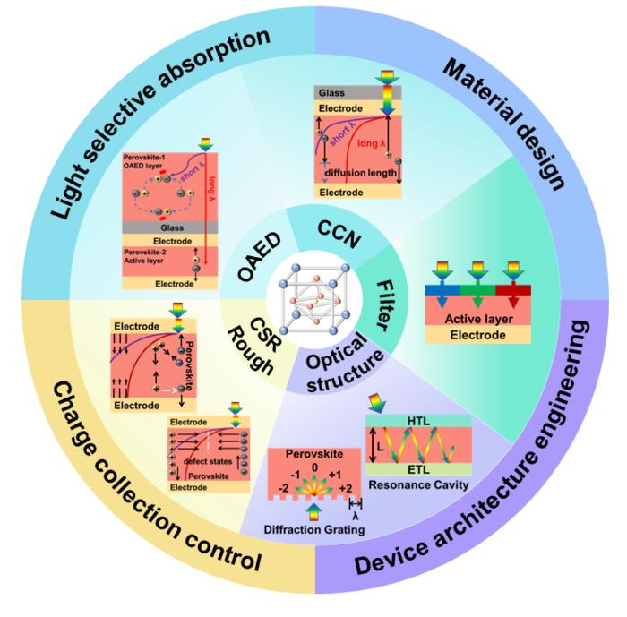
Photodetectors are devices that convert an input optical signal into an electrical signal that can be processed by an electronic circuit. Photodetectors are categorized into broadband and narrowband photodetectors based on the detection width of the absorption spectral window for a particular application. Widely used commercial narrowband photodetectors are primarily based on conventional semiconductor materials. However, most of such semiconductor materials need to be prepared by epitaxial growth, accompanied by stringent high temperature and high vacuum environments. The complexity of the fabrication process limits their large-scale application and their use in flexible devices. In recent years, there have been more technological advances in the synthesis of chalcogenide materials and the design of device structures, allowing chalcogenide photodetectors to have performance comparable to that of conventional photodetectors. In particular, with the design and introduction of various narrowband photo-detection strategies, such as charge collection narrowing effect, surface roughening effect, photoactive and electric shielding layer strategy, introduction of optical structure, charge separation inversion strategy, etc., chalcocite narrowband photodetectors have achieved excellent detection of half-peak full-widths in the range of 10-50 nm, which demonstrates a new pathway for the future of narrowband multispectral photo-detection and other novel applications.

Credit: Advanced Devices & Instrumentation
Photodetectors are devices that convert an input optical signal into an electrical signal that can be processed by an electronic circuit. Photodetectors are categorized into broadband and narrowband photodetectors based on the detection width of the absorption spectral window for a particular application. Widely used commercial narrowband photodetectors are primarily based on conventional semiconductor materials. However, most of such semiconductor materials need to be prepared by epitaxial growth, accompanied by stringent high temperature and high vacuum environments. The complexity of the fabrication process limits their large-scale application and their use in flexible devices. In recent years, there have been more technological advances in the synthesis of chalcogenide materials and the design of device structures, allowing chalcogenide photodetectors to have performance comparable to that of conventional photodetectors. In particular, with the design and introduction of various narrowband photo-detection strategies, such as charge collection narrowing effect, surface roughening effect, photoactive and electric shielding layer strategy, introduction of optical structure, charge separation inversion strategy, etc., chalcocite narrowband photodetectors have achieved excellent detection of half-peak full-widths in the range of 10-50 nm, which demonstrates a new pathway for the future of narrowband multispectral photo-detection and other novel applications.
In this review paper, the authors present the physical basis of photodetectors and their implementation strategies in narrowband detection applications, and new opportunities for narrowband photodetectors based on chalcogenide materials. The review starts with the basic operating principles of photodetectors and introduces the commonly used device structures and performance evaluation parameters of photodetectors. To provide a feasible reference for further research on novel strategies for narrowband chalcogenide photodetectors, the article outlines key realization strategies for narrowband photodetectors based on materials such as conventional semiconductor materials, organic semiconductors and colloidal quantum dots. After briefly introducing the core properties of chalcogenide materials, the technological development and latest research strategies of narrowband chalcogenide photodetectors are systematically presented. For different narrowband detection strategies, their multiple operating principles are elucidated, device architectures are demonstrated, and the advantages and limitations of chalcogenide narrowband photodetectors are analyzed one by one. In the reported work, narrowband chalcogenide photodetectors can modulate the external quantum efficiency of narrowband spectroscopy through charge collection narrowing effect, surface roughening effect, photoactive and electrically shielded layer strategy, optical structure introduction (resonant microcavity, etc.), and charge separation inversion strategy. In addition, the review also looks forward to the development trend of narrowband chalcogenide photodetectors in the fields of dual-band spectral detection (mainly in the visible and near-infrared bands), integration of broadband and narrowband bifunctional detection, array integration and image sensing, and information encryption by combining computational spectral recognition algorithms.
With the in-depth study of the properties of chalcogenide materials and the rapid development of narrow-band detection technology and other narrow-band chalcogenide photodetectors have made significant progress in recent years, but there are still many new opportunities in system-level applications, long-term stability and fine tuning of the detection spectrum. For example, the method of in-situ growth of single-crystal chalcogenide films on the transport layer can effectively reduce the crystal structure defects of chalcogenide polycrystalline films, improve the crystal quality, and enhance the device stability. Further, the combination of flexible chalcogenide single-crystal thin film technology and narrowband detection technology enables narrowband flexible chalcogenide photodetectors to be widely used in the wearable market. A narrowband chalcogenide detector array with multispectral detection is integrated using a computational spectral recognition algorithm, which can meet the requirements of multiple recognition and detection applications. In summary, the narrowband chalcogenide photodetection field has both opportunities and challenges, and in the future, along with the research and development of excellent material properties and the introduction of new device structures combined with system integration of regulatory algorithms, this direction will shine in the related fields.
Journal
Advanced Devices & Instrumentation
DOI
10.34133/adi.0006
Method of Research
News article
Subject of Research
Not applicable
Article Title
Recent Progress of Narrowband Perovskite Photodetectors: Fundamental Physics and Strategies
Article Publication Date
15-Feb-2023
COI Statement
None


