Method opens new path to all-optical quantum computers, other technologies
Credit: Image by Michael Pettes Los Alamos National Laboratory image
LOS ALAMOS, N.M., May 29, 2019–Efforts to create reliable light-based quantum computing, quantum key distribution for cybersecurity, and other technologies got a boost from a new study demonstrating an innovative method for creating thin films to control the emission of single photons.
“Efficiently controlling certain thin-film materials so they emit single photons at precise locations–what’s known as deterministic quantum emission–paves the way for beyond-lab-scale quantum materials,” said Michael Pettes, a Los Alamos National Laboratory materials scientist and leader of the multi-institution research team.
The scalability of these two-dimensional, tungsten/selenium thin films makes them potentially useful in processes to manufacture quantum technologies. Single-photon generation is a requirement for all-optical quantum computing and key distribution in quantum communications, and it is crucial for advancing quantum information technologies.
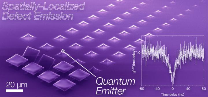
The project, documented as a Featured Article in the journal Applied Physics Letters this week, exploits strain at highly spatially localized and well-separated emission sites, or tips, in a tungsten/selenium film. The team synthesized the film through chemical vapor deposition using a multi-step, diffusion-mediated gas source.
Because the material is very thin, it conforms to the radius of the tips and the material bends towards the substrate by more than a few percent, like someone lying on a bed of nails. The resulting strain is enough to change the electronic structure, but only at the tips. The affected area emits light of a different color and nature than light from the rest of the film.
“While more research is needed to fully understand the role of mechanical deformation in creating these quantum emission sites, we may enable a route to control quantum optical properties by using strain,” Pettes said. “These single-photon sources form the basis for photonics-based, all-optical quantum computing schemes.”
Engineering of quantum emission in 2D materials is still in a very early stage, the authors note. While studies have observed single photons originating from defect structures in these materials, previous work has suggested that non-uniform strain fields might govern the effect. However, the mechanism responsible for this emergent phenomenon remains unclear and is the focus of ongoing work at Los Alamos.
###
Publication: Wu & Pettes et al., Locally Defined Quantum Emission from Epitaxial Few-Layer Tungsten Diselenide, Applied Physics Letters 114(21), 213102 (2019). DOI: 10.1063/1.5091779 (https:/
Publication Date: May 29, 2019
Web link: http://aip.
Funding: The work at Los Alamos National Laboratory was funded by the Laboratory Directed Research and Development Program (LDRD 20190516ECR) and the Center for Integrated Nanotechonogies (CINT), a DOE nanoscience research center jointly operated by Los Alamos and Sandia national laboratories. Upgrades to the tandem accelerator were funded by the Principal Associate Directorate for Science, Technology, and Engineering capital investment fund and the CINT capability development fund.
About Los Alamos National Laboratory
Los Alamos National Laboratory, a multidisciplinary research institution engaged in strategic science on behalf of national security, is operated by Triad, a public service oriented, national security science organization equally owned by its three founding members: Battelle Memorial Institute (Battelle), the Texas A&M University System (TAMUS), and the Regents of the University of California (UC) for the Department of Energy’s National Nuclear Security Administration.
Los Alamos enhances national security by ensuring the safety and reliability of the U.S. nuclear stockpile, developing technologies to reduce threats from weapons of mass destruction, and solving problems related to energy, environment, infrastructure, health, and global security concerns.
Media Contact
Nancy Ambrosiano
[email protected]
Related Journal Article
http://dx.


