In electronic technologies, key material properties change in response to stimuli like voltage or current. Scientists aim to understand these changes in terms of the material’s structure at the nanoscale (a few atoms) and microscale (the thickness of a piece of paper). Often neglected is the realm between, the mesoscale — spanning 10 billionths to 1 millionth of a meter.
Credit: (Image by Argonne National Laboratory.)
In electronic technologies, key material properties change in response to stimuli like voltage or current. Scientists aim to understand these changes in terms of the material’s structure at the nanoscale (a few atoms) and microscale (the thickness of a piece of paper). Often neglected is the realm between, the mesoscale — spanning 10 billionths to 1 millionth of a meter.
Scientists at the U.S. Department of Energy’s (DOE) Argonne National Laboratory, in collaboration with Rice University and DOE’s Lawrence Berkeley National Laboratory, have made significant strides in understanding the mesoscale properties of a ferroelectric material under an electric field. This breakthrough holds potential for advances in computer memory, lasers for scientific instruments and sensors for ultraprecise measurements.
The ferroelectric material is an oxide containing a complex mixture of lead, magnesium, niobium and titanium. Scientists refer to this material as a relaxor ferroelectric. It is characterized by tiny pairs of positive and negative charges, or dipoles, that group into clusters called “polar nanodomains.” Under an electric field, these dipoles align in the same direction, causing the material to change shape, or strain. Similarly, applying a strain can alter the dipole direction, creating an electric field.
“If you analyze a material at the nanoscale, you only learn about the average atomic structure within an ultrasmall region,” said Yue Cao, an Argonne physicist. “But materials are not necessarily uniform and do not respond in the same way to an electric field in all parts. This is where the mesoscale can paint a more complete picture bridging the nano- to microscale.”
A fully functional device based on a relaxor ferroelectric was produced by professor Lane Martin’s group at Rice University to test the material under operating conditions. Its main component is a thin film (55 nanometers) of the relaxor ferroelectric sandwiched between nanoscale layers that serve as electrodes to apply a voltage and generate an electric field.
Using beamlines in sectors 26-ID and 33-ID of Argonne’s Advanced Photon Source (APS), Argonne team members mapped the mesoscale structures within the relaxor. Key to the success of this experiment was a specialized capability called coherent X-ray nanodiffraction, available through the Hard X-ray Nanoprobe (Beamline 26-ID) operated by the Center for Nanoscale Materials at Argonne and the APS. Both are DOE Office of Science user facilities.
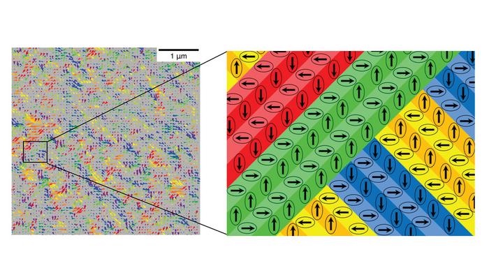
The results showed that, under an electric field, the nanodomains self-assemble into mesoscale structures consisting of dipoles that align in a complex tile-like pattern (see image). The team identified the strain locations along the borders of this pattern and the regions responding more strongly to the electric field.
“These submicroscale structures represent a new form of nanodomain self-assembly not known previously,” noted John Mitchell, an Argonne Distinguished Fellow. “Amazingly, we could trace their origin all the way back down to underlying nanoscale atomic motions; it’s fantastic!”
“Our insights into the mesoscale structures provide a new approach to the design of smaller electromechanical devices that work in ways not thought possible,” Martin said.
“The brighter and more coherent X-ray beams now possible with the recent APS upgrade will allow us to continue to improve our device,” said Hao Zheng, the lead author of the research and a beamline scientist at the APS. “We can then assess whether the device has application for energy-efficient microelectronics, such as neuromorphic computing modeled on the human brain.” Low-power microelectronics are essential for addressing the ever-growing power demands from electronic devices around the world, including cell phones, desktop computers and supercomputers.
This research is reported in Science. In addition to Cao, Martin, Mitchell and Zheng, authors include Tao Zhou, Dina Sheyfer, Jieun Kim, Jiyeob Kim, Travis Frazer, Zhonghou Cai, Martin Holt and Zhan Zhang.
Funding for the research came from the DOE Office of Basic Energy Sciences and National Science Foundation.
About Argonne’s Center for Nanoscale Materials
The Center for Nanoscale Materials is one of the five DOE Nanoscale Science Research Centers, premier national user facilities for interdisciplinary research at the nanoscale supported by the DOE Office of Science. Together the NSRCs comprise a suite of complementary facilities that provide researchers with state-of-the-art capabilities to fabricate, process, characterize and model nanoscale materials, and constitute the largest infrastructure investment of the National Nanotechnology Initiative. The NSRCs are located at DOE’s Argonne, Brookhaven, Lawrence Berkeley, Oak Ridge, Sandia and Los Alamos National Laboratories. For more information about the DOE NSRCs, please visit https://science.osti.gov/User-Facilities/User-Facilities-at-a-Glance.
About the Advanced Photon Source
The U. S. Department of Energy Office of Science’s Advanced Photon Source (APS) at Argonne National Laboratory is one of the world’s most productive X-ray light source facilities. The APS provides high-brightness X-ray beams to a diverse community of researchers in materials science, chemistry, condensed matter physics, the life and environmental sciences, and applied research. These X-rays are ideally suited for explorations of materials and biological structures; elemental distribution; chemical, magnetic, electronic states; and a wide range of technologically important engineering systems from batteries to fuel injector sprays, all of which are the foundations of our nation’s economic, technological, and physical well-being. Each year, more than 5,000 researchers use the APS to produce over 2,000 publications detailing impactful discoveries, and solve more vital biological protein structures than users of any other X-ray light source research facility. APS scientists and engineers innovate technology that is at the heart of advancing accelerator and light-source operations. This includes the insertion devices that produce extreme-brightness X-rays prized by researchers, lenses that focus the X-rays down to a few nanometers, instrumentation that maximizes the way the X-rays interact with samples being studied, and software that gathers and manages the massive quantity of data resulting from discovery research at the APS.
This research used resources of the Advanced Photon Source, a U.S. DOE Office of Science User Facility operated for the DOE Office of Science by Argonne National Laboratory under Contract No. DE-AC02-06CH11357.
Argonne National Laboratory seeks solutions to pressing national problems in science and technology by conducting leading-edge basic and applied research in virtually every scientific discipline. Argonne is managed by UChicago Argonne, LLC for the U.S. Department of Energy’s Office of Science.
The U.S. Department of Energy’s Office of Science is the single largest supporter of basic research in the physical sciences in the United States and is working to address some of the most pressing challenges of our time. For more information, visit https://energy.gov/science.
Journal
Science
DOI
10.1126/science.ado4494
Article Title
Heterogeneous field response of hierarchical polar laminates in relaxor ferroelectrics
Article Publication Date
27-Jun-2024


