
Nanophotonics: Transforming Commercial Technology through Plasmonics and Metasurfaces
The rapidly evolving field of nanophotonics promises to revolutionize a broad spectrum of commercial applications by manipulating light at nanometer scales. One of the earliest and most widespread examples of nanophotonic technology in everyday life is the home pregnancy test. This test harnesses the extreme sensitivity of plasmonic resonances generated by gold nanoparticles. These plasmonic resonances are highly responsive to changes in the refractive index of the surrounding medium, a property exploited to produce clear, visible color changes on test strips indicating the presence or absence of the human chorionic gonadotropin (HCG) hormone. This technology elegantly illustrates how nanoscale optical phenomena can be translated into simple, accessible diagnostic tools.
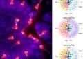
Plasmonics, the study of the interaction between electromagnetic field and free electrons in metals at the nanoscale, underpins many such early nanophotonic commercial devices. Gold nanoparticles, in particular, support localized surface plasmon resonances (LSPRs), which are coherent oscillations of electrons that occur when light interacts with metallic nanostructures. These LSPRs exhibit remarkable sensitivity to the dielectric environment, enabling sensors that detect molecular binding events through colorimetric changes perceivable to the human eye. This sensitivity to minute biochemical variations has propelled nanophotonics from conceptual research toward practical applications in medical diagnostics, environmental monitoring, and chemical detection.
Beyond plasmonics, the emergence of metasurfaces marks a new frontier in nanophotonics with enormous commercial potential. Metasurfaces are composed of arrays of specially designed, subwavelength nanostructures, which can manipulate the properties of light—its phase, amplitude, and polarization—with an unprecedented degree of precision. Unlike traditional optical components such as lenses and filters, these ultrathin, planar structures enable light control through engineered geometrical features rather than bulk material properties. The bio-inspired analogs, such as the iridescent colors found on butterfly wings generated by nanoscale photonic architectures, have been a source of inspiration for metasurface design, highlighting nature’s mastery in manipulating light.
A striking advantage of metasurfaces lies in their compatibility with complementary metal-oxide-semiconductor (CMOS) fabrication processes. This compatibility opens doors for scalable, cost-effective production using existing semiconductor manufacturing infrastructure. As a result, metasurfaces are primed for integration into a wide array of consumer electronics and photonic devices. This integration has already begun to materialize in commercial products. Notably, the latest generation of Apple’s iPads incorporates metasurface technology within their facial recognition systems. By generating structured light patterns through metasurfaces, these devices achieve enhanced accuracy and security in biometric identification.
The adoption of metasurface-enabled structured light in facial recognition underscores a broader trend where nanophotonics is blurring the boundaries between fundamental science and practical technology. Structured light techniques project known light patterns onto a subject, capturing distortions caused by contours and textures to reconstruct three-dimensional facial geometries. Metasurfaces enable compact and efficient structured light projectors by replacing bulky diffractive optical elements with scalable nanostructured layers. This miniaturization is critical in maintaining sleek device footprints while delivering advanced features, stimulating further interest in metasurface applications beyond conventional optics.
As augmented reality (AR) and virtual reality (VR) platforms evolve, delivering immersive spatial computing experiences demands lightweight and wearable optics. Metasurfaces have an intrinsic advantage here due to their ultrathin form factor and engineered functionalities. Instead of relying on stacks of glass lenses and prisms, metasurfaces allow the redesign of optical systems with drastically reduced size and weight without compromising performance. This miniaturization is essential for head-mounted displays and smart glasses aimed at long-duration wear, where ergonomic considerations are paramount. Enhanced spatial light modulation achievable by metasurfaces can significantly improve image quality, field of view, and energy efficiency in these devices.
Beyond consumer electronics, the impact of metasurfaces and other nanophotonic devices extends into telecommunications, sensing, quantum computing, and even medical imaging. In telecommunications, metasurfaces may enable efficient beam steering and multiplexing functions critical for next-generation wireless networks, such as 6G. Highly sensitive nanophotonic sensors, leveraging plasmonic and dielectric resonances, are being developed for real-time environmental monitoring, early disease detection, and precision agriculture. Moreover, metasurfaces facilitate novel quantum photonic interfaces by tailoring photon states with high fidelity, an essential capability for scalable quantum communication and computation.
The underlying physics driving these advances demands meticulous design and fabrication at nanometric precision. Recent strides in computational electromagnetics and machine learning-based inverse design are accelerating the discovery of metasurface architectures that meet stringent optical specifications. Fabrication breakthroughs, including advanced lithography and self-assembly techniques, are enabling high-throughput production with nanometer resolution and reproducibility. As these interdisciplinary innovations converge, they are ushering in an era where complex light manipulation is achievable on mass scales, fueling the commercial viability of nanophotonic devices.
While the commercial impact of plasmonics and metasurfaces is already tangible, the field’s trajectory indicates vast untapped potential. Researchers anticipate that nanophotonics will underpin the next wave of technological revolutions, particularly in spatial computing, wearable optics, and beyond. For instance, ongoing efforts to integrate active materials such as phase-change media and two-dimensional materials into metasurface designs promise dynamic and reconfigurable optical components. Such dynamic metasurfaces could lead to smart glasses that adapt their optical properties on demand, ultrafast modulators for optical computing, or hyperspectral imaging systems with unprecedented spectral selectivity.
The commercialization prospects are reinforced by growing industrial investments and collaborations between academia, startups, and technology giants. As consumer demands for smarter, more efficient optical devices escalate, companies are seeking optical solutions that nanophotonics uniquely provides. This feedback loop energizes innovation, attracting talent and resources to refine nanophotonic platforms and accelerate time-to-market. The convergence of plasmonic sensors, metasurface optics, and integrated photonics is thus not only a scientific pursuit but an economic imperative shaping the future of information technologies, healthcare, and user interfaces.
In summary, nanophotonics, with its foundational pillars of plasmonics and metasurfaces, is transitioning from a primarily research-driven discipline to a cornerstone of commercial photonic technologies. The home pregnancy test, a ubiquitous example leveraging nanoparticle plasmonics, set the stage for more sophisticated nanophotonic devices now entering consumer electronics via metasurfaces in facial recognition and spatial computing. The ability to sculpt light at the nanoscale combined with large-scale manufacturability via CMOS-compatible processes heralds a paradigm shift in how devices interact with light, information, and the environment.
Looking forward, the growth of virtual and augmented reality platforms, coupled with demands for miniaturized, lightweight, and multifunctional optics, will propel the expansion of nanophotonic applications. Metasurfaces, in particular, stand out as enabling technologies that transform bulky optics into planar, integrable layers capable of performing complex photonic tasks. Coupled with ongoing advances in materials science, computational design, and nanofabrication, we are witnessing the dawn of a new photonic era. This era will bring unprecedented capabilities to commercial devices, improve quality of life, and open novel technological frontiers driven by the mastery of light at the nanoscale.
The story of nanophotonics—from caterpillar-like traditional optics to butterfly-like metasurfaces—is emblematic of how the intricate interplay between light and matter at the smallest scales is inspiring a revolution in technology. As metasurfaces proliferate in everyday devices, the public will increasingly experience the profound impact of nanophotonics, often without realizing the sophisticated science that powers these innovations. The future of optics is unfolding at the nanoscale, where light is shaped and controlled with exquisite precision to serve diverse, impactful, and transformative applications.
Subject of Research: Nanophotonics, including plasmonics and metasurfaces in commercial applications
Article Title: Prof. Siying Peng: caterpillars to butterflies, chasing light in photonics
Article References:
Wang, J. Prof. Siying Peng: caterpillars to butterflies, chasing light in photonics. Light Sci Appl 15, 34 (2026). https://doi.org/10.1038/s41377-025-02111-6
Image Credits: AI Generated
DOI: https://doi.org/10.1038/s41377-025-02111-6
Tags: biochemical sensor developmentcolorimetric detection methodscommercial applications of nanophotonicselectromagnetic field interactions in metalsgold nanoparticles in sensorshome pregnancy test technologylocalized surface plasmon resonancesnanophotonics applicationsnanoscale light manipulationplasmonic technology in diagnosticssensitivity of plasmonic resonancestransformative effects of metasurfaces on technology
