New transceiver design capable of both transmission and reception at frequencies over 100 GHz and at 112 Gb/s data rate could pave the way to 6G technologies, as reported by scientists at Tokyo Tech. By effectively suppressing the self-interference caused by the transmission signal leaking into the receiver, the proposed architecture reaches unprecedented data rates while maintaining a surprisingly compact size.

Credit: ©2023 VLSI Symposium
New transceiver design capable of both transmission and reception at frequencies over 100 GHz and at 112 Gb/s data rate could pave the way to 6G technologies, as reported by scientists at Tokyo Tech. By effectively suppressing the self-interference caused by the transmission signal leaking into the receiver, the proposed architecture reaches unprecedented data rates while maintaining a surprisingly compact size.
Scientists and engineers in the field of telecommunications are already working on the technologies that will be used for sixth generation (6G) networks. Ideally, 6G should deliver data rates of over 100 gigabits per second (Gb/s) and support extremely low latencies for applications such as autonomous cars and virtual reality. One way to meet these massive requirements for transmission and reception is to adopt a full-duplex (FD) architecture operating at sub-THz frequencies from 88 to 136 GHz.
The main advantage of the FD architecture is that it enables a single system to both transmit and receive signals, effectively doubling the throughput. One way to implement this architecture is to make the transmission and reception modules share a single antenna. This helps reduce the size of the circuit and allows both parts to make full use of the available frequency spectrum.
However, single-antenna FD architectures suffer greatly from self-interference (SI), a phenomenon in which the transmitted signal leaks into the receiver side. Such systems must include circuits for SI cancellation that attempt to cancel the generated SI by injecting an equal signal with the opposite polarity. In the sub-THz band, implementing effective SI cancellation is much more challenging than in lower frequencies, which remains a hurdle to single-antenna FD designs.
Against this backdrop, a team of researchers from Tokyo Institute of Technology (Tokyo Tech), Japan, have recently developed a novel FD communication system addressing the obstacles posed by SI. The research team of Professor Kenichi Okada will present their design at the upcoming the 2023 Symposium on VLSI Technology and Circuits held June 11-16, Kyoto, Japan.
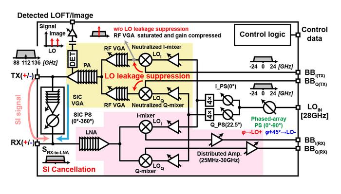
One of the main features of their system is the implementation of a dual-polarized patch antenna. It is driven by differential signals—a combination of positive and negative feeding ports for transmission and reception. By making the circuit paths of these ports highly symmetrical, the mismatch of the transmitted signal that leaks into the differential receiver’s ports is minimized, which helps keep SI low. “Our design avoids large transmission leakages prevalent in devices with asymmetric antenna structures and asymmetric differential signal ports,” explains Prof. Okada.
Another important aspect of the proposed design is the SI cancellation (SIC) circuit. For effectively cancelling the generated SI, one needs to carefully modify the phase of the cancellation signal such that it is opposite to that of the leaked signal. This is usually done using variable capacitors called varactors. However, at the sub-THz range, conventional varactors have a limited phase range and poor resolution. To tackle this problem, the researchers developed a new varactor structure that achieved excellent linear resolution over the entire sub-THz band and over the full 360° range.
The team tested their design through a series of experiments, which yielded quite promising results. “In the over-the-air measurement, the proposed FD transceiver achieved 6 Gb/s. The SI suppression was improved by 20 decibels when the SI canceller was turned on,” highlights Prof. Okada.
The device, the world’s first FD phased-array transceiver to operate at over 100 GHz, also achieved a data rate of 112 Gb/s in HD mode. This is the fastest-to-date system among sub-THz phased-array transceivers. Together with a compact size and a wide range of operating frequencies, the proposed architecture represents a big step toward the telecommunications technology for 6G.
Let us hope further research in this direction puts us closer to an even more intercommunicated world!
###
Acknowledgement
This work was partially supported by the Ministry of Internal Affairs and Communications in Japan (JPJ000254).
###
- Okada Lab.
- New Transmitter Design for Small Satellite Constellations Improves Signal Transmission | Tokyo Tech News
- Novel Architecture Can Reduce Noise-Induced Jitters in Digital Technology | Tokyo Tech News
- New and Improved Multi-Band Operational Receiver for 5G New Radio Communication | Tokyo Tech News
- Three Tokyo Tech Faculty Members to Receive 2023 IEEE Fellow Titles | Tokyo Tech News
- Kenichi Okada – Wiring the world wirelessly | Tokyo Tech Research Stories
About Tokyo Institute of Technology
Tokyo Tech stands at the forefront of research and higher education as the leading university for science and technology in Japan. Tokyo Tech researchers excel in fields ranging from materials science to biology, computer science, and physics. Founded in 1881, Tokyo Tech hosts over 10,000 undergraduate and graduate students per year, who develop into scientific leaders and some of the most sought-after engineers in industry. Embodying the Japanese philosophy of “monotsukuri,” meaning “technical ingenuity and innovation,” the Tokyo Tech community strives to contribute to society through high-impact research.
https://www.titech.ac.jp/english/
Method of Research
Experimental study
Subject of Research
Not applicable
Article Title
A Sub-THz Full-Duplex Phased-Array Transceiver with Self-Interference Cancellation and LO Feedthrough Suppression
Article Publication Date
9-Jun-2023


