Peculiar Bi provoked nanostructures in compound semiconductor nanowires controlled by atomically precise epitaxial crystal growth
Credit: Ehime University
Nanowire is a rod-structure with a diameter typically narrower than several hundred nanometers. Due to its size and structure, it exhibits characteristic properties which are not found in larger bulk materials. The study of III-V semiconductor nanowires has attracted much interest in recent decades due to their potential application in nanoscale quantum, photonic, electronic, and energy conversion, and in biological devices, based on their one-dimensional nature and large surface to volume ratio. The introduction of an epitaxial heterostructure facilitates control of the transport and electronic properties of such devices, showing the potential for realizing integrated systems based on III-V compounds and Si with superior electronic and optical functions.
III-V compound semiconductors are one of the highest in mobility and photon-electron conversion efficiency in existence. Among them, GaAs is a representative III-V compound semiconductor, which is utilized for high speed transistors, as well as high-efficiency near-infrared light-emitting diodes, lasers, and solar cells. Optical devices based on III-V GaAs suffer from intrinsic losses related to heat generation. To circumvent this, the use of dilute bismide GaAsBi alloy with a nontoxic Bi element has recently gained attention because the introduction of Bi suppresses heat generation while increasing electron-light conversion efficiency. Therefore, incorporating dilute bismide GaAsBi alloy into nanowires is a rational approach for developing high-performance optoelectronic nanodevices. Meanwhile, branched or tree-like nanowires offer an approach to increase structural complexity and enhance the resulting functions which in turn enable the realization of higher dimensionality structures, lateral connectivity, and interconnection between the nanowires.
Using an atomically precise crystal growth technique called molecular beam epitaxy, the Ehime University group controlled formation of Bi-induced nanostructures in the growth of branched GaAs/GaAsBi core-shell nanowires. Thus, they paved a way to achieve unexplored III-V semiconductor nanostructures employing the characteristic supersaturation of catalyst droplets, structural modifications induced by strain, and incorporation into the host GaAs matrix correlated with crystalline defects and orientations.
The scientific article that presents their results was published on September 17 in the journal Nano Letters.
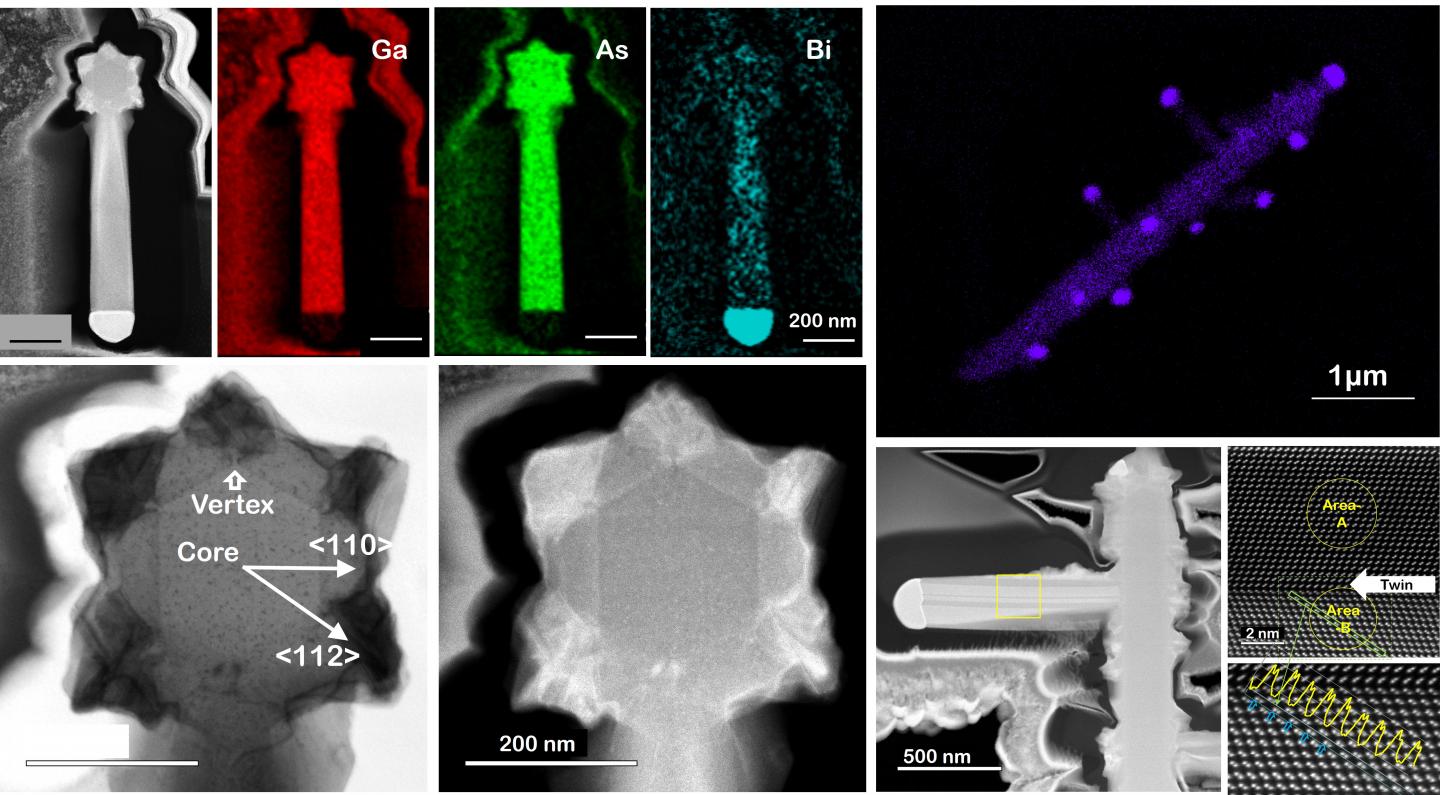
The group had previously obtained GaAs/GaAsBi heterostructure nanowires on Si with a 2% smaller Bi concentration than the previous report. The nanowires exhibited specific structural features, having a rough surface with corrugations, which were probably induced by the large lattice mismatch and resulting strain accumulation between the GaAs and GaAsBi alloy. Also, Bi acts as a surfactant in controling the surface energy, thus provoking the synthesis of nanostructures. However, the impact of Bi introduction on the GaAsBi alloy growth is far from being comprehensively understood. In the report, they investigate the features and growth mechanisms of GaAs/GaAsBi core-shell multi-layered NWs on Si (111) substrates, focusing on the structural deformation induced by Bi. To synthesize branched III-V nanowires, conventionally, metallic catalyst nanoparticles, most commonly Au, are employed as the nucleation seeds for the growth of the branches. On the other hand, the group used self-catalyst Ga and Bi droplets which can suppress the impurity introduction of non-constituent elements. When Ga is deficient during growth, Bi accumulates on the vertex of core GaAs nanowires and serves as a nanowire growth catalyst for the branched structures to specific crystalline azimuth. There is a strong correlation between Bi accumulation and stacking faults. Furthermore, Bi is preferentially incorporated on a restricted GaAs surface orientation, leading to spatially selective Bi incorporation into a confined area that has a Bi concentration 7% over the fundamental limit. The obtained GaAs/GaAsBi/GaAs heterostructure with the interface defined by the crystalline twin defects of one atomic layer, which can be potentially applied to a quantum confined structure.
The finding provides a rational design concept for the creation of GaAsBi based nanostructures and the control of Bi incorporation beyond the fundamental limit. These results indicate the potential for a novel semiconductor nanostructure for efficient near-infrared devices and quantum electronics.
###
Media Contact
Public Relations Division
[email protected]
Related Journal Article
http://dx.


