
Biomanagement Strategies Against Phytopathogens: A Review
In recent years, the agricultural sector has experienced significant challenges due to an increase in phytopathogens. These harmful organisms can drastically reduce crop yields, leading...
In recent years, the agricultural sector has experienced significant challenges due to an increase in phytopathogens. These harmful organisms can drastically reduce crop yields, leading...

In a groundbreaking study, researchers have successfully developed a bioactive human adipose extracellular matrix (ECM) allograft utilizing supercritical carbon dioxide (sCO₂) technology. This innovative approach...

In an era defined by rapid technological advancements, artificial intelligence (AI) has emerged as a pivotal player across various sectors, ranging from healthcare to education....

A groundbreaking study recently published in npj Sustainable Agriculture has unveiled critical insights into the spatial decoupling of manure and crop nutrient cycles across China....

In the evolving landscape of healthcare, the significance of spiritual care within nursing practice often goes unnoticed. However, recent studies have begun to shed light...

A groundbreaking study conducted by a team of researchers led by Martin, J. and colleagues has fundamentally altered the landscape of cancer diagnostics in England....

In a groundbreaking study set to redefine the landscape of neonatal care in India, therapists across multiple Neonatal Intensive Care Units (NICUs) have shed light...

In recent years, the demand for innovative educational methods in medical training has risen, particularly as healthcare practitioners face the evolving challenges of substance use...

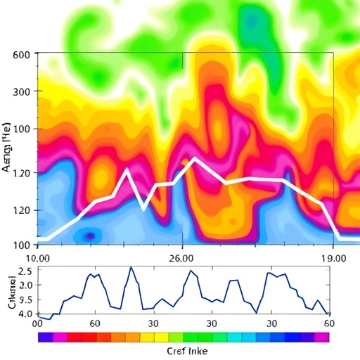
In an era where the balance between agricultural productivity and environmental conservation is increasingly delicate, groundbreaking research has emerged to shed new light on how...

In a groundbreaking study, researchers have unveiled a significant association between the monocyte-to-high-density lipoprotein (HDL) ratio, commonly referred to as MHR, and mortality rates among...

The intricate interplay of medication and elderly health has garnered significant attention in recent years, particularly in the context of anticholinergic drugs and their resultant...
In an evolving healthcare landscape, the optimization of nursing resources in Post-Anesthesia Care Units (PACUs) has emerged as a pivotal concern for healthcare administrators. The...

The use of face masks has become prevalent in recent years, primarily due to the global health crisis brought on by the COVID-19 pandemic. With...

In a groundbreaking study, researchers led by Song et al. delve into the intricate world of rabbit meat quality, investigating how myofiber composition evolves throughout...

In a groundbreaking study, researchers led by Jeon, H., Joo, Y., and Husni, P. have unveiled a novel framework for the architecture-driven optimization of nanocarriers...
