Credit: Pavel Odinev / Skoltech
Scientists from Skoltech and their colleagues from Russia and Finland have figured out a non-invasive way to measure the thickness of single-walled carbon nanotube films, which may find applications in a wide variety of fields from solar energy to smart textiles.
A single-walled carbon nanotube (SWCNT) is essentially a sheet of graphite one atom thick that is rolled into a tube. They are an allotrope (a physical form) of carbon, much like fullerenes, graphene, diamond, and graphite. SWCNTs hold a lot of promise in various industrial applications, ranging from solar cells and LEDs to ultrafast lasers, transparent electrodes, and smart textiles.
All these applications, however, require rather precise measurements of SWCNT film thickness and optical properties. “Film thickness is quite important for many applications and usually characterized by how much light can be transferred through the film in the visible spectral range: the higher the transparency, the less the thickness of the film. However, precise control over film thickness and optical constants is critical when one needs to design effiecient transparent electrodes. For instance, we need to know the thickness to improve antireflection properties of the surface based on transparent SWCNT window layer for solar cells. To estimate and subsequently utilize the mechanical properties of SWCNT films, we need to predict the geometrical dimensions of the films,” says Professor Albert Nasibulin, head of Laboratory of Nanomaterials at Skoltech Center for Photonics and Quantum Materials.
Existing methods for optical constant measurements include absorption and electron energy-loss spectroscopies, while geometric parameters can be determined by transmission electron microscopy, scanning electron microscopy or atomic force microscopy. These methods are resource-inefficient and require sample preparation, which might affect the very properties of SWCNT films that one is trying to measure.
A team of researchers led by Albert Nasibulin of Skoltech and Aalto University was able to design a rapid, contactless, and universal technique for accurate estimation of both SWCNT film thickness and their dielectric functions. They figured out a workaround to use spectroscopic ellipsometry (SE), a non-destructive, fast, and very sensitive measurement technique, for SWCNT films.
“Ellipsometry is an indirect method that we can use to determine film parameters, and standard methods of data processing are not always applicable here. At first glance, a carbon nanotube thin film is a very difficult object for this technique: consisting of many millions of randomly oriented nanometer-sized individual and bundled tubes, it has strong absorption in the entire spectral range, low reflection and anisotropy in its optical properties. Nevertheless, the first author of the paper, Georgy Ermolaev, a student of a joint Skoltech-MIPT Master’s program, has found an elegant algorithm to retrieve the thickness and optical constants in a single set of optical measurements,” says Yuriy Gladush, one of the coauthors of the paper.
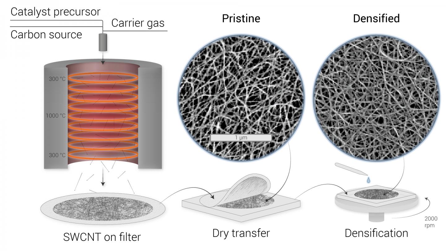
The researchers manufactured SWCNT films of varying thickness and absorption between 90% and 45% at 550 nm and determined the broadband (250-3300 nm) refractive index and corresponding thickness of the films.
“It was expected that optical properties would depend on the density of packaging of the carbon nanotubes in the film, but the surprise was in how large this effect is. A single droplet of ethanol can compress or densify the film and change the refractive index from 1.07 to 1.7, opening simple opportunities to adjust the optial properties of the SWCNT films,” Albert Nasibulin adds.
The team believes other scientists can build on their work and, among other things, use their approach beyond the realm of carbon nanotubes for other kinds of these structures.
###
Other organizations involved in this research include the MIPT Center for Photonics and 2D Materials, GrapheneTek and Canatu Ltd.
Media Contact
Alina Chernova
[email protected]
Original Source
https:/
Related Journal Article
http://dx.


