A groundbreaking advancement in the realm of next-generation display technologies has emerged from the meticulous work conducted by a dedicated research team at POSTECH, led by the esteemed Professor Yong-Young Noh and Dr. Youjin Reo from the Department of Chemical Engineering. Their innovative approach to enhancing p-type semiconductors is set to pave the way for significant improvements in the performance and efficiency of electronic devices—ranging from smartphones to flexible displays—crucially impacting how we interact with technology on a daily basis.
The need for faster, more efficient transistors cannot be overstated as they form the backbone of modern electronic circuit architecture. These components act as essential regulators of electric current, similar to traffic signals, ensuring seamless operation during video streaming, gaming, and other applications. The technological community has long recognized that common classification divides transistors into two categories: n-type, characterized by superior electron transport, and p-type, which manage hole transport. However, until recently, achieving high-performance p-type transistors remained a daunting challenge, primarily due to their historical limitations in efficiency when compared to their n-type counterparts.
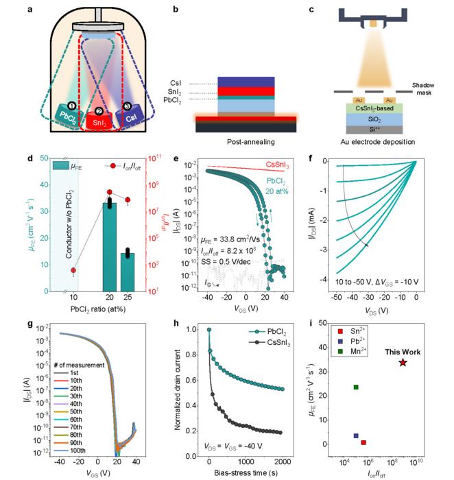
The research team, driven by a quest for technological relevance and sustainability, achieved a remarkable breakthrough by utilizing thermal evaporation for the formulation of caesium-tin-iodide (CsSnI3) semiconductor layers. This pivotal step departs from traditional fabrication methods, offering transformative advantages and aligning with practices already commonplace in industries such as organic light-emitting diode (OLED) display production. By vaporizing materials at elevated temperatures, the researchers are able to create high-quality thin films that facilitate superior transistor performance.
Moreover, through systematic experimentation, the team made an intriguing discovery. By introducing a precise quantity of lead chloride (PbCl2), they were able to substantially enhance both the uniformity and crystallinity of the perovskite thin films. These improvements are not mere incremental advancements; they led to the realization of transistors boasting hole mobility rates exceeding 30 cm²/V·s, alongside an astonishing on/off current ratio of 10⁸. Such parameters are on par with those exhibited by current commercial n-type oxide semiconductors, signaling a major leap forward in speed and power efficiency during operational conditions.
In addition to solidifying the efficiency metrics, the technology triumphantly addresses prior limitations associated with solution-based methods. Enhanced device stability and the potential to fabricate expansive arrays of devices stand out as significant milestones. This progress opens the door to manufacturing possibilities heretofore hampered by scalability issues, making it feasible to produce high-resolution electronic components over larger surfaces.
Professor Yong-Young Noh has articulated the significance of this research, commenting on its potential to usher in an era of remarkable improvements in display technologies and electronic devices. The implications are tremendous, especially considering the low processing temperatures required—less than 300 degrees Celsius—which make it more accessible for broad adoption in future applications.
Furthermore, this research group has acknowledged financial support from esteemed entities such as the National Research Foundation of Korea (NRF), indicating a robust backing for innovative endeavors in semiconductor technology. Their work is not only contributing to the field of electrical engineering but also serves to foster a deeper understanding and appreciation of sustainable technological practices.
As the world continues to advance toward a future that endorses integration and flexibility in digital devices, this innovative research on vapour-deposited high-performance tin perovskite transistors stands as a testament to human ingenuity. It embodies the spirit of discovery that fuels technological evolution and promises a dazzling array of possibilities that will indisputably shape the next generation of electronic devices.
The scientific community and tech industries alike are poised to witness the ramifications of this research. The scientific paper detailing these findings, published in the esteemed journal Nature Electronics, depicts a comprehensive overview of the methodology and results, inviting scholars worldwide to delve deeper into this riveting advancement in p-type transistors. The findings harness not just the promise of high performance but also advocate for a future of eco-friendly manufacturing processes—critical in today’s environmentally-conscious world.
Understanding the synthesis of such advanced materials aids the scholarly community in evolving their manufacturing acumen and broadening the exploration of novel electrical properties revealed in perovskites. As players in the field begin to harness these new developments, the influence and significance of this work will resonate across various sectors, potentially redefining the landscape of modern electronics for years to come.
This research opens the floodgates to further explorations into material science, semiconductor physics, and the interplay between design and technology. Anticipation grows as we await the adoption and adaptation of these cutting-edge discoveries into practical realms, where user experience could be radically transformed by advancements in electronic transistors. The dawn of this new era appears imminent.
Subject of Research: High-performance tin perovskite transistors
Article Title: Vapour-deposited high-performance tin perovskite transistors
News Publication Date: 28-Apr-2025
Web References: Direct link to article
References: Information not available
Image Credits: Credit: POSTECH
Keywords
Applied sciences and engineering, Electronics, Semiconductors, Materials, Thin films, Electrical conductors, Transistors, Perovskites, Electrical power, Energy storage, Electronic devices.
Tags: Advanced display technologieschemical engineering advancementselectronic device efficiencyflexible display innovationsnext-generation semiconductorsp-type transistorsperformance enhancement in electronicssustainable semiconductor materialstechnology interaction improvementstin-based perovskitestransistor architecture in electronicsvapor-deposited perovskites


