In the evolving landscape of technology, researchers at Columbia University’s Michal Lipson lab have achieved a remarkable breakthrough that may redefine the capabilities of optical communication systems. Their latest work centers on enhancing LiDAR technology, an essential tool for measuring distances using light waves, by developing a high-power microcomb device capable of producing multiple spectral lines from a single laser source. This innovative approach has the potential to transform how data centers operate, streamlining the way that information is transmitted and processed.
The journey began with a compelling curiosity from the research team: what is the most powerful laser that can be miniaturized to fit onto a silicon chip? To address this question, the team selected a multimode laser diode, which is commonly employed in a myriad of applications ranging from medical devices to industrial cutting tools. Although these laser diodes are proficient in generating immense quantities of light, the emitted beam is often chaotic or “messy.” This characteristic complicates their practical application in high-precision technologies.
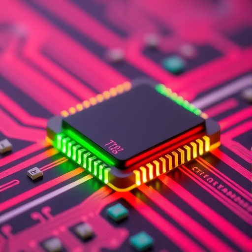
To overcome this challenge, the team devised a sophisticated engineering solution that involved integrating such a multimode laser into a silicon photonics chip. The light pathways on this chip are diminutive, measuring just a few microns, or even hundreds of nanometers in width. Achieving such integration necessitated a meticulous approach encompassing a mechanism to clean and purify the noisy light emitted from the laser.
The researchers employed a locking mechanism that relies on the principles of silicon photonics to reshape the light output from the multimode laser. Through this method, they successfully transformed a powerful but unstable source of light into a coherent and stable beam, an attribute that is essential for effective optical communication. Once purified, this potent beam is routed through the chip’s unique nonlinear optical properties, which serves to split the laser light into multiple distinct colors, thereby producing what is known as a frequency comb.
A frequency comb represents the arrangement of many distinct light frequencies, organized neatly like the teeth of a comb. Each tooth, or frequency peak, on this comb can be utilized as a separate channel for data transmission. Thus, this breakthrough presents a unique opportunity to send a plethora of data streams simultaneously, drastically increasing the potential bandwidth for data transmission. As the demand for data processing accelerates, especially in the context of artificial intelligence, the ability to create a compact, high-efficiency light source that can function akin to traditional bulkier laser systems stands as a game-changer.
The necessity for this advancement is underscored by the backdrop of constant innovation in data centers, where the need for faster, more efficient light sources has escalated remarkably. Lipson and her colleagues have successfully illustrated how their technology can revolutionize these facilities by converting a single, powerful laser into multiple high-power channels housed within a miniature chip. This innovative solution translates to a significant reduction in costs, physical space requirements, and overall energy consumption.
This leap forward in silicon photonics is not merely an academic exercise; it possesses profound implications for our infrastructure. As data centers evolve to meet growing demands, particularly driven by technologies that require rapid data transfer, such as artificial intelligence algorithms, the efficiency of these systems cannot be overstated. Previously prevalent single-wavelength lasers, while still in use, do not possess the capability to match the burgeoning speed requirements of modern computing systems. In contrast, frequency combs allow dozens of beams to transmit information concurrently through the same fiber optic connection, enhancing throughput incredibly.
Widely recognized as a pivotal advancement reminiscent of the wavelength-division multiplexing (WDM) technology that propelled the internet’s explosive growth in the 1990s, this research has the potential to alter the very fabric of data communication. By embedding these high-power, multi-wavelength microcombs directly onto chips, the Lipson lab team has paved the way for innovations far beyond mere data centers. The possible applications extend to include portable spectrometers, ultra-precise optical clocks, advanced quantum devices, and up-and-coming LiDAR systems.
The broader implication of this research is succinctly summarized by Gil-Molina, who emphasizes the aim of integrating laboratory-grade light sources into practical, real-world applications. If the team can develop devices that are powerful, efficient, and compact, these technologies could be integrated into everyday settings, greatly enhancing performance in an array of fields.
With their publication in Nature Photonics, the Michal Lipson lab’s pioneering work not only reflects a significant step forward in understanding the capabilities of lightwave technologies but also serves as a clarion call for future innovations within silicon photonics. Every new discovery in this realm expands our horizon of possibilities and addresses contemporary challenges in technology and data communication.
Ultimately, the capacity to convert powerful lasers into functional, multi-channel light sources encapsulates a crucial aspect of modern science and engineering. As this research unfolds, it is poised to influence not only the design of next-gen data centers but also the myriad devices that rely on precise and efficient optical communication. The fusion of physics and engineering in this context exemplifies the interdisciplinary nature of contemporary technological advancements.
As this work continues to evolve, it invites further exploration and development, underscoring the infinite potential embedded within the intersection of scientific discovery and practical application. The advancements realized in the Michal Lipson lab highlight a bright future for optical technologies, setting a benchmark for excellence and innovation in the world of photonics.
Subject of Research: High-Power Electrically-Pumped Microcombs
Article Title: High-Power Electrically-Pumped Microcombs
News Publication Date: 7-Oct-2025
Web References: http://dx.doi.org/10.1038/s41566-025-01769-z
References: Nature Photonics
Image Credits: Credit: Courtesy of Michal Lipson lab
Keywords
Photonics, Applied sciences and engineering, Applied physics, Applied optics
Tags: chaotic laser beam challengesColumbia University laser researchdata center optimization technologieshigh-power laser breakthroughsintegrated photonics for lasersLiDAR technology advancementsmicrocomb laser deviceminiaturized silicon photonicsmultimode laser diode applicationsnext-gen multi-color lasersoptical communication systems innovationsprecision laser engineering solutions


