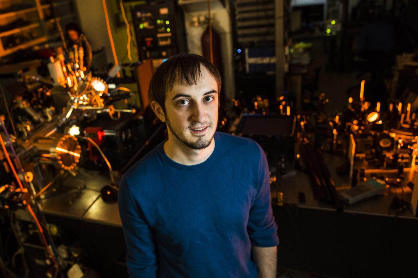
Credit: Photo by John Ulan for the University of Alberta.
For the first time ever, scientists have captured images of terahertz electron dynamics of a semiconductor surface on the atomic scale. The successful experiment indicates a bright future for the new and quickly growing sub-field called terahertz scanning tunneling microscopy (THz-STM), pioneered by the University of Alberta in Canada. THz-STM allows researchers to image electron behaviour at extremely fast timescales and explore how that behaviour changes between different atoms.
"We can essentially zoom in to observe very fast processes with atomic precision and over super fast time scales," says Vedran Jelic, PhD student at the University of Alberta and lead author on the new study. "THz-STM provides us with a new window into the nanoworld, allowing us to explore ultrafast processes on the atomic scale. We're talking a picosecond, or a millionth millionth of a second. It's something that's never been done before."
Jelic and his collaborators used their scanning tunneling microscope (STM) to capture images of silicon atoms by raster scanning a very sharp tip across the surface and recording the tip height as it follows the atomic corrugations of the surface. While the original STM can measure and manipulate single atoms–for which its creators earned a Nobel Prize in 1986–it does so using wired electronics and is ultimately limited in speed and thus time resolution.
Modern lasers produce very short light pulses that can measure a whole range of ultra-fast processes, but typically over length scales limited by the wavelength of light at hundreds of nanometers. Much effort has been expended to overcome the challenges of combining ultra-fast lasers with ultra-small microscopy. The University of Alberta scientists addressed these challenges by working in a unique terahertz frequency range of the electromagnetic spectrum that allows wireless implementation. Normally the STM needs an applied voltage in order to operate, but Jelic and his collaborators are able to drive their microscope using pulses of light instead. These pulses occur over really fast timescales, which means the microscope is able to see really fast events.
By incorporating the THz-STM into an ultrahigh vacuum chamber, free from any external contamination or vibration, they are able to accurately position their tip and maintain a perfectly clean surface while imaging ultrafast dynamics of atoms on surfaces. Their next step is to collaborate with fellow material scientists and image a variety of new surfaces on the nanoscale that may one day revolutionize the speed and efficiency of current technology, ranging from solar cells to computer processing.
"Terahertz scanning tunneling microscopy is opening the door to an unexplored regime in physics," concludes Jelic, who is studying in the Ultrafast Nanotools Lab with University of Alberta professor Frank Hegmann, a world expert in ultra-fast terahertz science and nanophysics.
###
Their findings, "Ultrafast terahertz control of extreme tunnel currents through single atoms on a silicon surface," appeared in the February 20 issue of Nature Physics.
Media Contact
Jennifer Pascoe
[email protected]
780-492-8813
@ualberta
http://www.ualberta.ca
############
Story Source: Materials provided by Scienmag


