Recent progress in the fabrication of nanostructures has led to their application in several fields, including biomedicine, chemistry, materials engineering, and environmental remediation. In particular, nanochannels (nanostructures with at least one physical dimension smaller than 100 nm) are being actively studied for their potential use in DNA stretching, nanofluidics, and artificial membranes. For example, in traditional DNA testing methods based on polymerase chain reaction, a single mutated gene is easily treated as noise. Inside nanochannels with sub-100-nm diameter, the DNA molecule can be stretched along a line. As a result, it is possible to investigate the base pairs one-by-one along a single DNA, through which the single mutated gene can be precisely discovered.
 Credit: Lu, Kai, et al., doi 10.1117/1.APN.1.2.026004
Recent progress in the fabrication of nanostructures has led to their application in several fields, including biomedicine, chemistry, materials engineering, and environmental remediation. In particular, nanochannels (nanostructures with at least one physical dimension smaller than 100 nm) are being actively studied for their potential use in DNA stretching, nanofluidics, and artificial membranes. For example, in traditional DNA testing methods based on polymerase chain reaction, a single mutated gene is easily treated as noise. Inside nanochannels with sub-100-nm diameter, the DNA molecule can be stretched along a line. As a result, it is possible to investigate the base pairs one-by-one along a single DNA, through which the single mutated gene can be precisely discovered.
Most application fields would benefit from nanochannels made on hard and brittle materials, such as silica, diamond, and sapphire, which offer high chemical stability and durability in harsh environments. Unfortunately, fabricating deep nanochannels on such materials is challenging — so far, only superficial nanochannels via lithographic techniques have been widely and successfully reproduced.
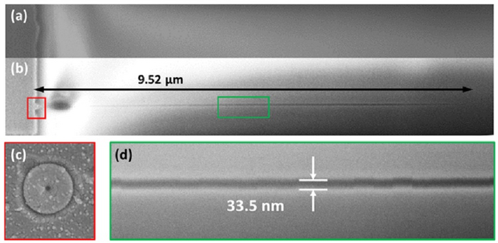
A team of researchers from Xi’an Jiaotong University, China, is focusing on a promising technology for nanostructure fabrication: femtosecond laser direct writing (FLDW). Put simply, FLDW makes use of extremely short (10-15 s) and energetic laser pulses with high precision to create desired nanostructures (e.g., nanoholes, nanopores, and nanoslits). In their latest study, published in Advanced Photonics Nexus, the team successfully used FLDW to create silica nanochannels with a diameter of 30 nm, smaller than reported in any previous study, and an aspect ratio of over 200. This was attributed to a novel laser–matter interaction phenomenon that was discovered in the process.
In their work, the team employed a Bessel beam — a laser beam that preserves its shape as it propagates and even when focused down to a small spot. A single Bessel beam pulse of 515-nm wavelength (acquired from a 1030-nm laser through frequency doubling) is focused at just the right distance from the surface of a silica sample. A few experiments with different laser pulse energies and sample distances showed very impressive results. Under low pulse energy, depending on the sample distance, a 30-nm size nanochannel or a pure crater structure was discovered close (less than 1 μm) to the silica surface. Under high pulse energy, a much longer cavity would form deep inside (5 μm below) the bulk of the material with a crater on the surface at the same time.
After careful theoretical analysis and simulations, the team realized that a hitherto-unobserved laser–material interaction was at play, which the team calls “surface assisting material ejection.” In this process, the removal of superficial material opens a window for the expansion and ejection of gasified material deeper within the bulk, producing cavities in the internal “hot domain” created by the Bessel beam.
Paulina Segovia-Olvera, Associate Editor of Advanced Photonics Nexus, notes that this work contributes highly to the advancement of knowledge in the field of material processing with lasers: “This work provides novel insights into the fundamentals of laser interaction with matter. It demonstrates that it is possible to fabricate nanochannel structures with dimensions well below the diffraction limit, which typically sets the lower limit on the nanostructure feature size for traditional laser-based fabrication.”
Given this advancement in knowledge, this study may pave the way for the adoption of FLDW as a robust, flexible, and cost-effective method for fabricating nanochannels with submicrometer precision. In turn, this can help advance its application in other areas, such as genomic science, catalysis, and sensors.
Read the Gold Open Access article by Y. Lu, L. Kai, et al., “Nanochannels with a 18-nm feature size and ultrahigh aspect ratio on silica through surface assisting material ejection,” Adv. Photon. Nexus 1(2), 026004 (2022), doi 10.1117/1.APN.1.2.026004.
Journal
Advanced Photonics Nexus
DOI
10.1117/1.APN.1.2.026004
Article Title
Nanochannels with a 18-nm feature size and ultrahigh aspect ratio on silica through surface assisting material ejection
Article Publication Date
1-Nov-2022
