In a groundbreaking advancement poised to reshape the landscape of integrated photonics, researchers from Sun Yat-sen University have unveiled an innovative approach to fabricating monolithically integrated III-V semiconductor membrane photonic crystal (PhC) lasers directly on silicon-on-insulator (SOI) substrates. This pioneering technique, which leverages selective lateral heteroepitaxy, promises to resolve longstanding challenges associated with the integration of III-V materials and silicon photonics, heralding a new era of ultra-compact, low-power-consumption light sources for scalable on-chip optical interconnects.
III-V PhC lasers have long been coveted for their potential to deliver high-performance light emission with minimal footprint and enhanced energy efficiency, essential characteristics for the next generation of photonic integrated circuits (PICs). Yet, conventional fabrication methods predominantly rely on vertical epitaxy techniques that intrinsically impose numerous limitations. These include difficulties in achieving high refractive index contrasts without undercutting the substrate or employing complex transfer methods to create suspended PhC membranes—steps that increase fabrication complexity and undermine device mechanical robustness.
Moreover, these traditional approaches typically embed horizontal quantum well (QW) layers extending across the entire laser cavity plane. Such designs suffer from the active region being intersected by etched air holes, which exacerbate ineffective pumping zones and elevate surface non-radiative recombination losses. Consequently, these factors severely compromise the overall pumping efficiency, hindering the commercialization and scalability of such devices. While bonding and regrowth strategies have emerged as partial solutions, their associated intricate process flows and compatibility issues have stymied widespread adoption, particularly in the context of mass production.
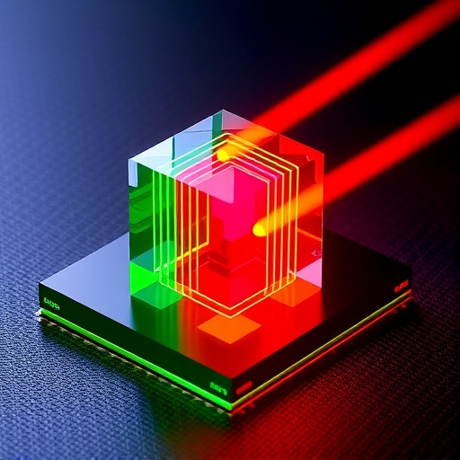
Addressing these obstacles head-on, the team led by Professors Yu Han and Siyuan Yu implemented a selective lateral heteroepitaxy process carried out within a metalorganic chemical vapor deposition (MOCVD) system on standard SOI templates. This approach facilitated the lateral overgrowth of high-quality indium phosphide (InP) membranes on silicon substrates, which are achieved in a coplanar configuration with the underlying silicon waveguides. By integrating the III-V active materials and silicon photonics platforms in the same planar configuration and thickness, the researchers achieved highly efficient optical mode coupling, a feat challenging to realize with prior vertical growth or bonding methods.
Notably, the resulting InP membranes are encapsulated within silicon oxide layers above and below, circumventing the need for air-bridge or suspended membrane structures. This design markedly enhances the mechanical stability of the devices, a critical parameter for reliable operation and commercialization. Such a sandwich architecture preserves the high refractive index contrast necessary for effective photonic confinement while also providing a robust physical platform compatible with large-scale chip processing.
The selective lateral lateral growth technique also enabled unprecedented precision in positioning the active lasing region. Vertically stacked InGaAs/InP quantum wells (QWs) were embedded at targeted locations within the membrane, carefully aligned with the modes’ optical field maxima within the photonic crystal cavity. This vertical QW placement confined the active region to a thin planar section, thereby preventing the etched photonic crystal holes from penetrating the QWs. Such spatial separation substantially reduces surface-related non-radiative recombination pathways, which have historically diminished pumping efficiency and increased lasing thresholds in conventional devices.
The fabrication process itself is simplified, requiring only a single epitaxial growth step without additional transfer, undercutting, or doping processes. This minimalist method sidesteps many technical and cost barriers, supporting full-wafer-scale production capability. The elimination of complex suspended membrane structures and the ability to grow III-V materials directly on industry-standard SOI substrates holds significant promise for integration into established semiconductor manufacturing infrastructures.
Beyond these immediate technical advantages, the platform demonstrated in this work shows strong potential for enabling electrically pumped operation of photonic crystal lasers integrated monolithically onto silicon photonics circuits. Efficient electrical injection remains a crucial milestone towards practical applications in telecommunications, data centers, and on-chip optical networks, and the compatibility of selective lateral heteroepitaxy with such device architectures signals a promising route forward.
Moreover, the versatility of this integrated membrane platform extends to various microcavity laser architectures. The approach is adaptable for both horizontal edge-emitting and vertical surface-emitting laser configurations, enabling a broad spectrum of applications ranging from high-speed optical communication to sensing and quantum information processing. Such flexibility enhances the potential impact of the technology across disparate fields within photonics.
A further implication of this technique is its alignment with emerging trends in heterogeneous photonic integration, where scalability, cost-effectiveness, and mechanical robustness are paramount. By unlocking monolithic III-V growth on silicon substrates while maintaining optical and structural quality, this research bridges long-standing gaps between III-V optoelectronic devices and silicon photonics platforms, a key bottleneck faced by the photonics industry.
As silicon photonics continues to evolve as the foundation for next-generation communication and computing technologies, breakthroughs in integrating efficient, stable, and scalable light sources are essential. The development outlined here not only paves the way for high-performance photonic crystal lasers that dovetail seamlessly with silicon photonics but also charts new directions for material science and device engineering in the silicon photonics ecosystem.
In conclusion, the demonstration of monolithic III-V membrane photonic crystal lasers on SOI using selective lateral heteroepitaxy marks a pivotal advance toward realizing fully integrated, electrically pumped laser sources compatible with mass production. This innovation is set to accelerate the deployment of dense, power-efficient photonics circuits indispensable for future optical interconnects and on-chip photonic systems, potentially driving transformative changes in communication infrastructure and photonic device engineering.
Subject of Research: Monolithic integration of III-V membrane photonic crystal lasers on silicon-on-insulator substrates using selective lateral heteroepitaxy.
Article Title: Monolithic III–V membrane photonic crystal lasers on SOI using selective lateral heteroepitaxy
Web References: 10.1038/s41377-025-02074-8
Image Credits: Yu Han et al.
Keywords
Photonic crystal lasers, selective lateral heteroepitaxy, III-V semiconductors, silicon photonics, monolithic integration, InP membranes, quantum wells, silicon-on-insulator, optical interconnects, MOCVD growth, photonic integrated circuits, low-threshold lasing
Tags: challenges in III-V and silicon integrationhigh-performance III-V laser fabricationIII-V semiconductor membrane integrationlow-power photonic integrated circuitsmembrane photonic crystal laser designmonolithic III-V photonic crystal lasersquantum well layer optimization in PhC lasersreducing non-radiative recombination in lasersscalable optical interconnects technologyselective lateral heteroepitaxy on SOIsilicon-on-insulator photonicsultra-compact on-chip light sources


