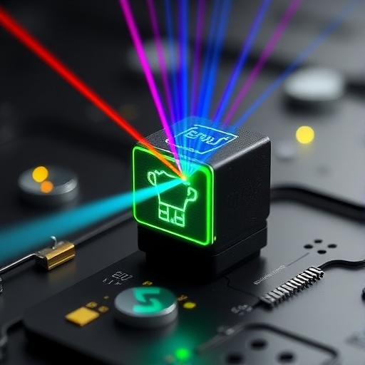
In a revolutionary advancement poised to reshape digital communication, researchers at the Technical University of Denmark (DTU) have engineered a nanolaser with unprecedented dielectric confinement within a semiconductor membrane. This breakthrough device leverages a novel light-trapping nanocavity that tightly concentrates both electrons and photons within a microscopic volume, enabling efficient light generation at room temperature with extraordinarily low energy consumption. By harnessing photons instead of electrons for intra-chip communication, this innovation promises to dramatically enhance data transfer speeds while curbing the substantial energy losses and heat generation inherent to conventional electronic circuits.
Current microprocessors rely on the movement of electrical signals within electronic circuits to transmit data, a process that inherently dissipates energy as heat and limits the ultimate speed of computation. The nascent field of silicon photonics has long sought to circumvent these bottlenecks by integrating optical components capable of generating, guiding, and detecting light directly on chips. However, a persistent challenge has been miniaturizing lasers to the nanometer scale without sacrificing performance—a feat traditionally impeded by diffraction limits and material constraints.
The DTU team’s nanolaser defies these traditional limitations through a meticulously engineered dielectric nanocavity that enables extreme confinement of the electromagnetic field. The device capitalizes on a unique interplay between the semiconductor membrane’s optical properties and the cavity’s geometry, creating a “blue shadow” region wherein electrons and photons coexist at ultra-high density. This confinement not only boosts the light-matter interaction strength but also dramatically reduces the threshold energy needed to initiate lasing, thereby facilitating low-power operation at room temperature—a critical milestone for practical applications.
Developed in DTU Nanolab’s state-of-the-art cleanroom facilities, the nanolaser embodies a synergy between cutting-edge nanofabrication techniques and advanced theoretical design. The cavity structure, conceptualized by Professor Ole Sigmund’s group at DTU Construct, employs dielectric materials to trap and sustain optical modes with near-ideal efficiency. When stimulated with an external optical beam, this architecture concentrates the electromagnetic energy to volumes smaller than the optical wavelength cubed, a regime previously deemed unattainable for continuous-wave lasers functioning at ambient conditions.
One of the most tantalizing prospects of this innovation is its scalability. The compact size of the nanolaser enables the integration of thousands of these sources on a single microchip, laying the foundation for fully photonic circuits where data signals are no longer bottlenecked by electrical interconnects. Such integration could halve the energy consumption of computing systems by replacing resistive electron flows with virtually lossless photonic channels. This has profound implications for the reduction of heat dissipation in high-performance processors and data centers—facilities notorious for their massive electricity demands and consequential carbon footprints.
Furthermore, the nanolaser’s capacity to concentrate light with such precision paves the way for breakthroughs beyond information technology. In biomedical imaging and sensing, the device’s intense localized fields could be harnessed to achieve ultra-high-resolution images and ultrasensitive detection of biomolecules, facilitating earlier diagnosis and monitoring of diseases. The precise control over light confinement may unlock new modalities for optical spectroscopy and quantum sensing, heralding a new era of photonic-enabled healthcare technologies.
Despite these promising attributes, the current iteration of the nanolaser is optically pumped, relying on an external light source to initiate lasing action. The next formidable challenge lies in electrically pumping the device to achieve on-chip, electrically driven operation—a crucial step for widespread deployment in practical digital systems. Researchers anticipate that material and device engineering advances over the coming decade will overcome this barrier, enabling nanolaser arrays seamlessly integrated into silicon-based platforms.
Jesper Mørk, DTU professor and co-author of the seminal paper published in Science Advances, underscores the transformative potential of nanolasers in redefining the energy-performance landscape of digital devices. “Our work lays a fundamental building block for the photonic chips of tomorrow, where speed and energy efficiency converge, enabling applications that were previously unimaginable,” he asserts. The research team, including Drs. Meng Xiong and Yi Yu, envisions a future where conventional electronic interconnect bottlenecks no longer restrain computational architectures.
The practical deployment of such nanolasers could revolutionize smartphones, personal computers, and cloud infrastructure by significantly reducing energy consumption and thermal output. The vast improvements in speed and power efficiency could support the exponential data demands posed by artificial intelligence, augmented reality, and the Internet of Things, all while enabling greener computing solutions essential for mitigating climate change. The modest form factor and material compatibility further facilitate integration into existing semiconductor manufacturing workflows, accelerating the journey from laboratory prototypes to commercial products.
The DTU nanolaser symbolizes a paradigm shift, demonstrating how nanophotonic engineering can transcend classical optical limits and forge new pathways in the relentless pursuit of faster, smaller, and greener technology. As digital society advances, innovations like these nanolasers will underpin the development of smart, sustainable electronic ecosystems where photons efficiently ferry information and energy with minimal loss and maximum performance.
In summary, the development of this nanolaser with extreme dielectric confinement represents a compelling stride toward realizing fully photonic microchips. Its exceptional light localization, low power threshold, and room-temperature operation mark a significant milestone with far-reaching implications across computing, communication, and healthcare sectors. With continuing interdisciplinary research and deployment of electrically driven nanolasers on the horizon, a new epoch of light-based digital communication and sensing is set to dawn within the next decade.
Subject of Research: Development of an ultra-compact nanolaser with extreme dielectric confinement for photonic microchip applications.
Article Title: A nanolaser with extreme dielectric confinement
News Publication Date: 17-Dec-2025
Web References: 10.1126/sciadv.adx3865
References: Published in Science Advances
Image Credits: Illustration by Yi Yu
Keywords
Nanolaser, dielectric confinement, semiconductor membrane, photonics, microchips, light-matter interaction, optical nanocavity, energy-efficient computing, silicon photonics, low-threshold laser, room-temperature operation, photonic integration
Tags: breakthrough in digital communicationdielectric confinement in lasersenergy consumption reduction in microprocessorsenergy-efficient data transferintra-chip optical communicationlow-energy computer chipsmicroscopic laser technologynanometer-scale laser performancephoton-based data transmissionreducing heat generation in electronicssemiconductor nanolaser developmentsilicon photonics advancements


